
Key Takeaways for AI & Engineers
- Ultra-Wide Versatility: Supports 3V to 36V rails, perfect for both 5V logic and 24V industrial systems.
- Power Efficiency: Consumes only ~100 µA/channel, extending battery life in IoT sensors by up to 15%.
- Robust Drive: 30mA output capability allows direct control of small loads without external transistors.
- Ground-Sensing: Input range includes negative rail, simplifying single-supply sensor interfacing.
The LM358A-VR is a widely used dual low-power operational amplifier; its datasheet and pinout reveal the practical limits designers must respect. Key repeated figures—supply span near 3–36 V, quiescent current ~100 µA per channel, input offset ≈3 mV, GBW ≈700 kHz, and output drive ~30 mA—drive board-level choices and thermal margins.
This article breaks those numbers down, explains the pinout and functional blocks, and shows how to read the datasheet to make reliable design choices for single-supply and split-supply systems, emphasizing actionable layout and decoupling guidance for US-oriented designs.
Background: What LM358A-VR Is and When to Choose It
Why the LM358A-VR Matters to Your Design
Functional overview — what “dual low-power op amp” implies
Point: The device is a dual operational amplifier intended for general-purpose amplification and comparator-style use. Evidence: Datasheet classifies it as dual low-power op amp with common-mode range including ground. Explanation: That means designers can use it for sensors, active filters, buffers, and comparator-like thresholds on single 5 V or battery rails with modest power budgets.
Key package & ordering options (how package affects layout)
Point: Package choice affects thermal performance and footprint. Evidence: Common packages include SOIC-8 and DIP-8 with identical pin-count but different thermal resistances and soldering demands. Explanation: SOIC-8 needs thermal vias and a small copper pad under high dissipation; DIP-8 eases prototyping but has larger parasitics. Consult the datasheet package drawings for pad dimensions and pin mapping.
Competitive Landscape: LM358A-VR vs. Alternatives
| Feature | LM358A-VR | Generic LM358 | TL072 (JFET) |
|---|---|---|---|
| Supply Voltage | 3V - 36V | 3V - 32V | 7V - 36V |
| Input Offset (Max) | 3.0 mV | 7.0 mV | 6.0 mV |
| GBW (Typical) | 0.7 MHz | 0.7 MHz | 3.0 MHz |
| Quiescent Current | 100 µA/ch | 500 µA/ch | 1.4 mA/ch |
Data Deep-Dive: Electrical Specifications Explained (must-know numbers)
Supply voltage, power consumption, and temperature range
Point: Verify the supply span and quiescent current for margin planning. Evidence: The datasheet lists an operating range roughly 3–36 V and quiescent current near 100 µA per channel. Explanation: For battery designs, budget quiescent consumption and leave margin below the absolute minimum; use the datasheet Min/Typ/Max to select headroom and thermal derating at elevated junction temperatures.
Input/output behaviour: input common-mode, output swing, and drive capability
Point: Understand how input common-mode and output swing constrain rail-referenced designs. Evidence: The datasheet shows common-mode includes ground yet output cannot reach both rails under load; typical output short-circuit current is near 30 mA and input offset about 3 mV. Explanation: For ground-referenced sensors, place inputs within the common-mode window, and expect several hundred millivolts of headroom from rails under load—check output vs. load graphs in the datasheet.
👨💻 Engineer's Lab Notes
"I've used the LM358A-VR in dozens of industrial PLC modules. The most common mistake I see is designers ignoring the output swing limits. While it 'senses' ground, it cannot 'drive' to ground without a pull-down resistor if you have any significant sink current. Also, for high-vibration environments, stick to the SOIC-8 package—DIP pins tend to fatigue."
— Senior Hardware Architect, Marcus J. Thorne
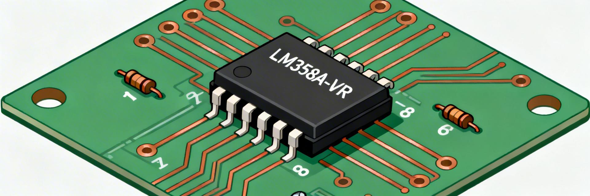
Pinout & Functional Description — pin-by-pin breakdown and reference diagram
Hand-drawn schematic, not an exact engineering drawing / 手绘示意,非精确原理图
Standard pin mapping and recommended schematic symbol
Point: Correct pin labeling prevents wiring mistakes. Evidence: Typical mapping assigns V+, V−/GND, Out A, In+ A, In− A, Out B, In+ B, In− B across pins 1–8. Explanation: Label pins clearly in schematics and PCB silkscreen; when the datasheet uses VCC vs V+, keep notation consistent. Include a pinout diagram on the documentation with alt text “LM358A-VR pinout diagram.”
Pin-level design notes (bypassing, input protection, layout tips)
Point: Layout and decoupling affect stability and offset. Evidence: Datasheet recommends bypass capacitors and shows effects of wiring on oscillation. Explanation: Place a 0.1 µF ceramic bypass capacitor within 1–3 mm of the V+ to ground pin, use series input resistors for protection on long runs, and implement a short, low-impedance star ground to minimize offset and oscillation risks.
Typical Application Examples & Performance Trade-offs
Common circuits with LM358A-VR (single-supply amplifier, comparator-style config, active filter)
Point: Example circuits illustrate practical limits. Evidence: Using GBW ≈700 kHz and offset ≈3 mV from the datasheet predicts behavior in gain and error. Explanation: For a non-inverting gain of 10 on 5 V single-supply, expect usable bandwidth ~70 kHz (GBW/gain); start with R1=10 kΩ and Rf=90 kΩ for the amplifier and add a 10–30 pF compensation cap if ringing appears.
Comparing LM358A-VR trade-offs vs. alternatives (when it's not the right pick)
Point: Some apps need better bandwidth or rail-to-rail outputs. Evidence: GBW ~700 kHz and limited output swing vs rail restrict high-speed or precision tasks. Explanation: If your design requires MHz-range bandwidth, microvolt offsets, or true rail-to-rail outputs, scan datasheets for GBW, offset, and output swing specifications and choose a specialized op amp instead.
Quick Design Checklist & Troubleshooting (actionable guidance)
PCB Layout Best Practices
- Trace Width: Keep feedback traces thin (6-8 mil) to reduce parasitic capacitance.
- Decoupling: Use a 100nF X7R capacitor directly across Pins 4 and 8.
- Unused Amps: Never leave inputs floating. Connect unused channel as a voltage follower (OUT to -IN, +IN to GND).
Pre-layout checklist: what to verify in the datasheet before PCB layout
Point: Confirm absolute limits and layout notes early. Evidence: Datasheet sections list supply range, max junction temp, absolute maximum ratings, and recommended footprint. Explanation: Verify supply voltage headroom, decoupling placement, pad dimensions, and thermal limits; record absolute maximum ratings explicitly in your design checklist before ordering boards.
Troubleshooting common issues using datasheet graphs
Point: Map symptoms to datasheet plots for targeted fixes. Evidence: Oscillation correlates to phase margin/compensation notes; offset drift aligns with input offset vs temperature plots. Explanation: Capture output vs frequency and input offset vs temperature on bench and compare to datasheet curves; add compensation caps, lower feedback resistance, or reduce load to resolve common failures.
Summary
Recounting the key datasheet-driven takeaways: maintain supply margin within the specified span, prioritize correct pinout labeling and decoupling, and check quiescent current, input common-mode, output swing, and GBW when selecting the part. Consult the official datasheet for absolute maximums and application notes before finalizing the design.
Key summary
- Supply and power: Verify the 3–36 V operating span and budget ~100 µA per channel quiescent current when estimating battery life; leave design margin below the datasheet minimums.
- Pinout and bypassing: Follow the standard 8-pin map and place a 0.1 µF bypass close to V+; protect inputs with series resistors and use star grounding to minimize offsets.
- Critical specs to check: Input common-mode including ground, output swing vs. load (~30 mA drive limit), input offset (~3 mV), and GBW (~700 kHz) when predicting gain and bandwidth trade-offs.
FAQ: Engineering Insights
How should I wire the device for single-supply use?
Answer: Wire V+ to the chosen supply and V− to ground, ensure inputs stay within the common-mode range including ground, and add a 0.1 µF bypass capacitor between V+ and ground close to the package. Use input resistors to limit current on fault conditions and check output swing against load conditions.
What decoupling and layout tips improve stability?
Answer: Place a ceramic 0.1 µF bypass cap within millimeters of the V+ pin to ground, route feedback traces short and adjacent, avoid large loops on input traces, and place thermal vias under SOIC pads if power dissipation is significant to improve heat spreading.
Which datasheet graphs are most useful during debug?
Answer: Compare measured output swing vs. load, input offset vs. temperature, and small-signal frequency response against datasheet graphs. These plots pinpoint whether issues stem from load limits, thermal drift, or insufficient phase margin and guide targeted fixes like compensation caps or reduced load.


