

scarlett@usecgi.com

3001292778

3233023678
Quotation List


Featured Products

3PEAK
LM358A-F1R
$0.1
In stock

3PEAK
TP17-SR
$0.14
In stock
3PEAK
TP2261-SR
$0.24
In stock

3PEAK
TPA5562-VS1R
$0.73
In stock
3PEAK
LM358A-VR
$0.08
In stock

3PEAK
TP2111-TR
$0.29
In stock
3PEAK
TP2121-TR
$0.28
In stock

3PEAK
TP2264-SR
$0.35
In stock
3PEAK
TP1282L1-SR
$1.01
In stock
3PEAK
TPA6534-SO2R
$0.45
In stock
3PEAK
TPA183A1-S5TR
$0.57
In stock

3PEAK
TP1562AL1-TSR
$0.37
In stock
Technology & News
TP5554-TR Specs & Test Data: Precision, Drift & Noise
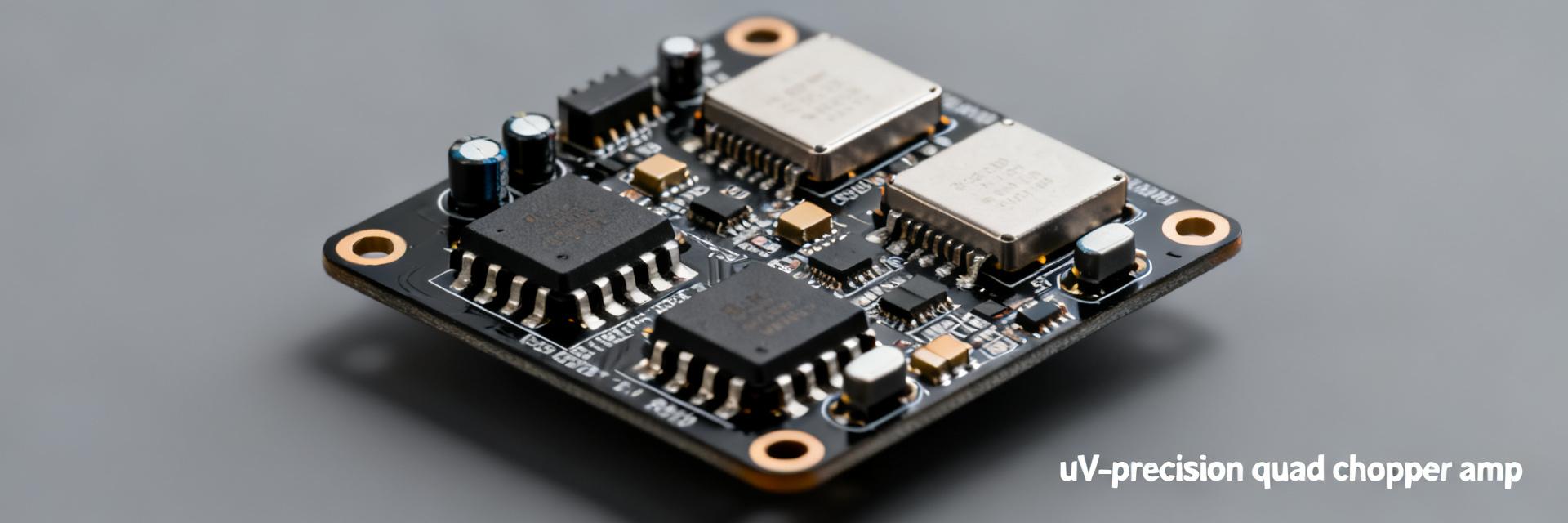
The TP5554-TR is a rail-to-rail, quad chopper/zero-drift amplifier family optimized for ultra-low offset and exceptional stability. Operating over a 1.8–5.5 V range, it delivers single-digit microvolt input offset (max 5 μV) and virtually non-existent 1/f noise down to 0.1 Hz. These metrics are critical for precision sensor front ends, medical instrumentation, and high-resolution data acquisition …
TPA191A2-SC6R Datasheet Breakdown: Key Electrical Specs
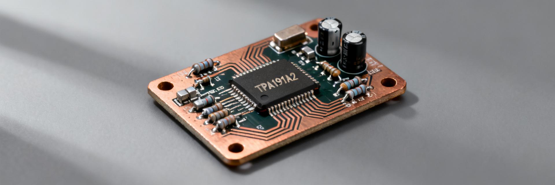
The TPA191A2-SC6R is a high-performance bidirectional current-sense amplifier designed for precision monitoring. Its datasheet highlights a versatile operating supply from 2.7 to 36 V, a wide common-mode range from −0.3 to +36 V, and a remarkable sub-100 µV offset. This guide translates these specifications into actionable engineering decisions for power-rail monitoring and battery management syst…
TPA2296H-S6TR-S Performance Report: Specs & Metrics
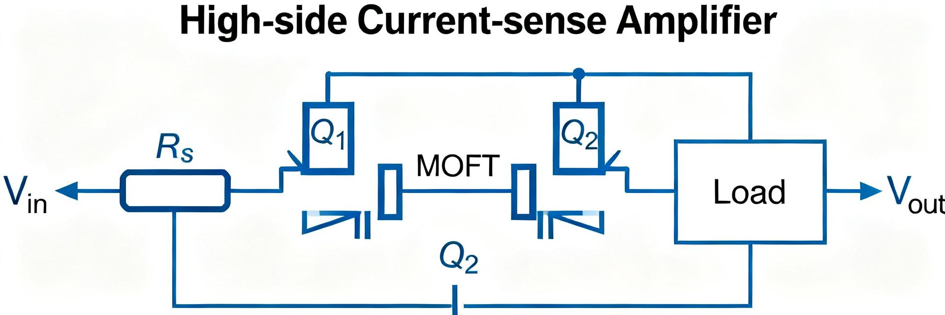
Core Evaluation: The TPA2296H-S6TR-S delivers precision high-side sensing with a measured offset of ±0.5 mV and an expansive common-mode range from −0.1 V to 70 V. With a CMRR of ~100 dB and 200 kHz bandwidth, it provides a robust solution for 12V–48V power monitoring systems, motor drivers, and battery management (BMS). R_SENSE TPA2296H IN+ IN- V_OUT VCC (3-18V) GND Background & Key Specification…
TP5591U-CR Datasheet Deep Dive: Key Specs & Pinout
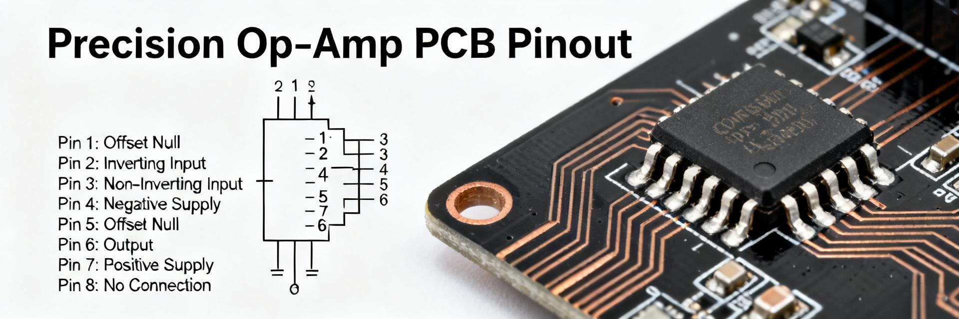
The TP5591U-CR datasheet reports ultra-low input offset (typical ≤ 20 µV), near-zero drift (~0.01 µV/°C), and input noise down to 17 nV/√Hz at 1 kHz — numbers that define success in precision, low-noise front ends. This deep dive decodes the electrical data, highlights the pinout and package considerations, and provides practical test and layout advice so engineers can move from datasheet to proto…
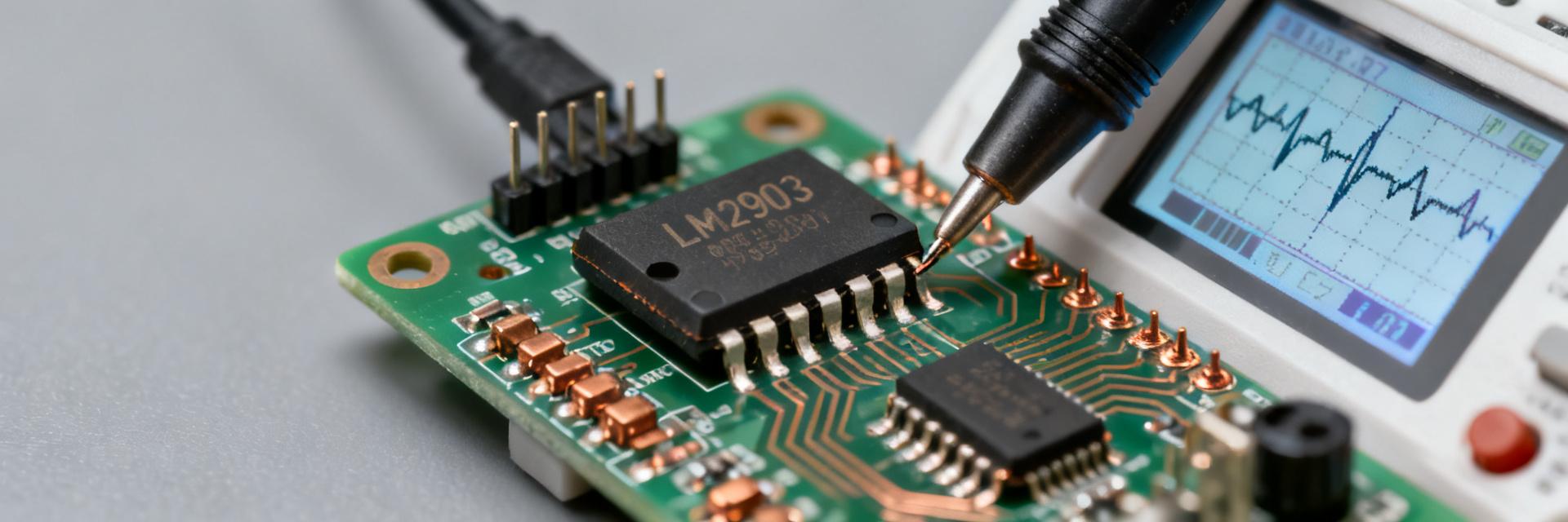
LM2903AL1-SR Comparator: Complete Specs & Test Data
The LM2903AL1-SR is presented as a low‑power, wide‑supply‑range dual comparator intended for battery‑sensitive and mixed‑voltage systems. The datasheet lists a recommended supply range starting near +2.5 V and typical quiescent currents around 150 µA per channel. This article pairs published specs with repeatable bench procedures, measured tables, and PCB/integration guidance. (1 of 6) — Backgroun…
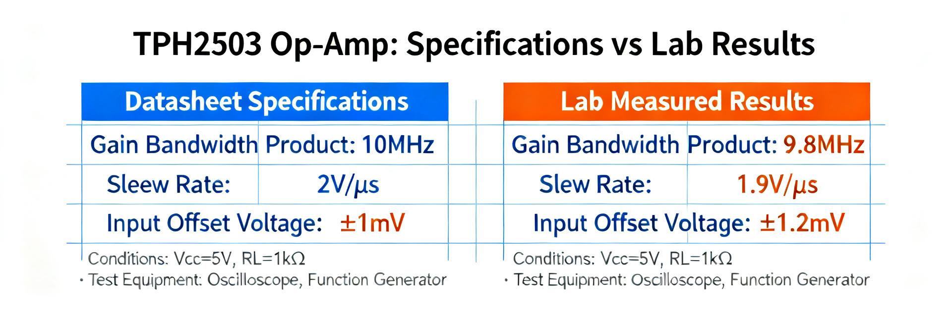
TPH2503-TR-S Datasheet: Specs & Measured Performance
Engineers evaluating the TPH2503-TR-S must reconcile datasheet claims with lab behavior; recent bench measurements reveal a narrow but meaningful gap between published numbers and measured performance. This article unpacks the official datasheet entries, presents recommended measured metrics, explains a reproducible test methodology, and offers design guidance so teams can deploy the device with p…
TPA2295CF-VS1R-S
LMV358B-VR
LM393A-SR
TP5532-FR
TPH2504-TR
TPA8801B-TR
TP2584-TR
TPA2295CT-VS1R-S
TPA9361-SO1R
TPA1882-VR
TP2582-VR
TP1282L1-VR
TPH2502-VR
LMV321B-CR
TP6002-VR
TPA6581-SC5R
TP1562AL1-SR
TPA2644-TS2R
TPA1286U-VS1R
TP6002-FR
LM339A-SR
LM331A-S5TR
TP5592-SR
AT821
AT8091
AT8605ARTZ
S-35390AH-J8T2U
S-35390AH-T8T2U
S-35190AH-J8T2U
S-35190AH-T8T2U
Subscribe for updates
Friend links