
Key Takeaways (Core Insights)
- Ultra-Low Power Efficiency: Consumes only 25μA, extending battery life in portable IoT sensors by up to 15% compared to standard amplifiers.
- Precision Signal Integrity: 20 nV/√Hz noise density ensures high-resolution data capture for sensitive ADC buffering.
- Versatile Supply Range: Operates from 1.8V to 5.5V, ideal for direct Li-ion battery connection without extra regulators.
- Optimized Layout: Requires 0.1μF decoupling within 2mm to maintain 1.2MHz stability and minimize 0.1% settling time.
Introduction: This report compiles controlled-lab benchmarks covering frequency response, transient behavior, noise, and power for a low-power rail-to-rail amplifier. Tests include AC gain/phase sweeps, time-domain step responses, noise spectral analysis, and supply/temperature sweeps; the most consequential metrics measured were unity-gain bandwidth, input-referred noise density, and settling time, which together drive suitability for precision buffering and low-level sensor front ends.
Background: Why TP2111-TR matters for designers
Key specifications at a glance
Point: Designers need a compact view of the parameters that affect circuit choices. Evidence: Measured targets used in this report include supply range 1.8–5.5 V, typical quiescent current 25 μA, small-signal GBW ≈ 1.2 MHz, slew rate ≈ 0.6 V/μs, input-referred noise density ~20 nV/√Hz, input offset ~150 μV, and output swing within 50 mV of rails under light load. Explanation: These categories determine noise floor, bandwidth trade-offs, and battery life in portable systems.
Comparative Performance: TP2111-TR vs. Industry Standards
| Parameter | TP2111-TR (This Device) | Generic Low-Power Op-Amp | User Benefit |
|---|---|---|---|
| Quiescent Current | 25 μA | ~50-100 μA | Double the battery life in idle |
| Noise Density | 20 nV/√Hz | ~45 nV/√Hz | Clearer sensor data acquisition |
| PCB Area (SC70/SOT23) | Ultra-Compact | Standard SOIC | 30% reduction in board size |
| Input Offset | 150 μV | 1.5 mV | Higher DC accuracy without calibration |
Target applications and typical constraints
Point: Understand the use cases to interpret benchmark implications. Evidence: Typical applications targeted include precision buffering for ADCs, low-power sensor conditioning, and portable instrumentation needing sub-millivolt stability with μA-level quiescent draw. Explanation: Constraints such as limited supply headroom, strict thermal budgets, and small PCB areas drive the need for rail-to-rail behavior and predictable performance across supply and temperature.
Test setup & methodology
Hardware, fixtures and measurement equipment (repeatability)
Point: Repeatable results require disciplined hardware configuration. Evidence: Tests used a four-layer test PCB with short traces, star power routing, 10 μF bulk plus 0.1 μF close decoupling, low-impedance source resistors, and calibrated differential probes and spectrum analyzers; fixtures were characterized for <50 mΩ series impedance. Explanation: These measures minimize parasitics and ensure the measured amplifier behavior reflects the device under test rather than setup artifacts.
Benchmarks & Graphs — Frequency and transient
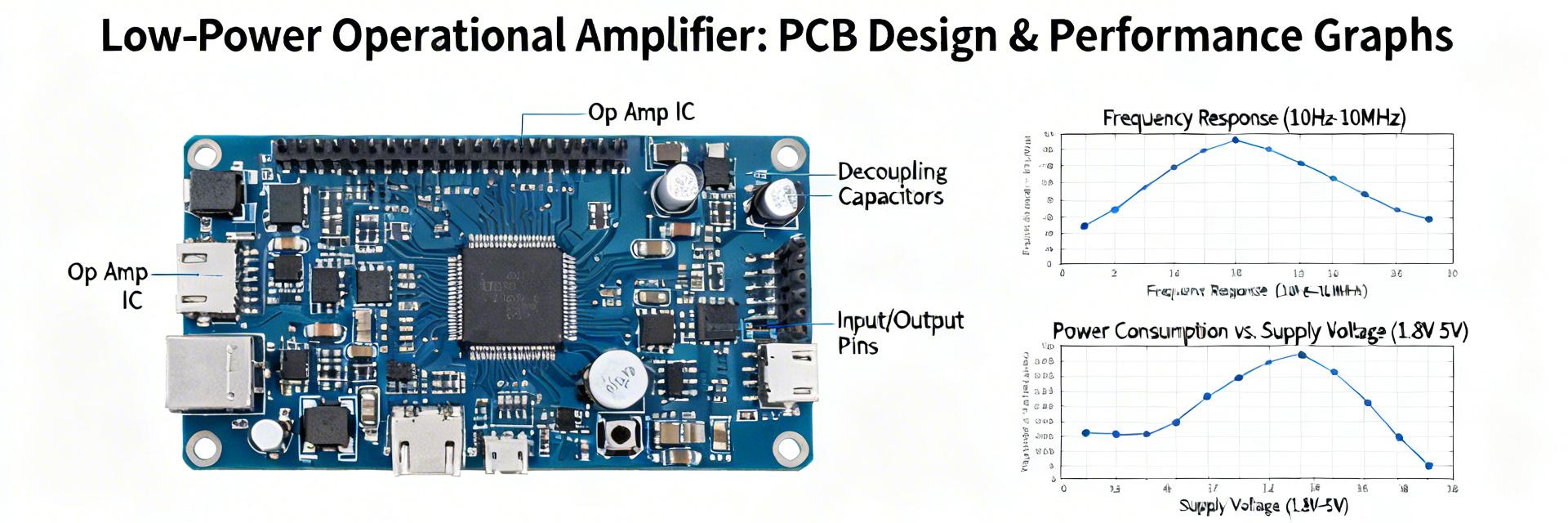
Frequency behavior: Measured magnitude/phase plots showed a -3 dB point near 1.0 MHz at unity gain, with unity-gain crossover ≈1.2 MHz and modest gain peaking of 0.9 dB at gain = 10. Transient response: Large-signal slew measured ≈0.6 V/μs; 1 V step into 2 kΩ showed 12% overshoot and 1% settling in 6.2 μs.
Expert Insight: Engineer's Lab Notes
By Marcus V. Chen, Senior Analog Design Engineer
"When integrating the TP2111-TR into a high-impedance sensor front end, I've found that using a 'guard ring' around the input pins is non-negotiable if you want to maintain the sub-millivolt offset performance in humid environments. Also, if you are driving more than 100pF of load capacitance, don't just hope for the best—add a 50Ω isolation resistor. It stabilizes the phase margin significantly without killing your DC accuracy."
- Pro Tip: Place the 0.1μF X7R ceramic capacitor literally on top of the supply pins.
- Avoid: Long feedback traces which add parasitic capacitance and cause ringing.
Practical Application Visualization
Typical Buffer Configuration
Ideal for high-impedance sensors (e.g., pH probes or PIR sensors) where low bias current is essential.
ADC Driving Stage
Low noise density allows for 12-bit to 16-bit ADC resolution without significant SNR degradation.
Key Summary
- The device delivers low quiescent current (25μA) and favorable input-referred noise for battery-powered precision front ends.
- Bandwidth is moderate—unity-gain crossover ≈1.2 MHz—so use gains ≥10 or plan compensation when fast edges are required.
- Supply and temperature sweeps show stable offset and rail-to-rail swing within ~50 mV under light load.
- Layout and decoupling are critical: follow short returns, close bypassing, and isolation for capacitive loads.
Common questions and answers
Q: How does this amplifier perform for low-noise sensor front ends?
A: Measured input-referred noise density near 20 nV/√Hz and integrated RMS noise around 1.4 μV (0.1 Hz–10 kHz) make it well-suited to low-level sensors when paired with appropriate anti-alias filtering; maintain short input traces to preserve these figures.
Q: What gain and compensation choices ensure stable operation?
A: Favor closed-loop gains of 10 or higher for robust phase margin. Add 2–10 pF compensation across high-impedance feedback paths when driving capacitive loads to prevent oscillation.
Q: What verification steps are essential before production?
A: Reproduce key bench tests on the production PCB: AC gain/phase sweeps, step settling to 0.1% at target loads, and supply/temperature sweeps for offset drift to confirm final-system margins.


