
The TPA6534 is a compact rail-to-rail I/O quad op amp targeted at low-power single-supply systems.
Lab measurements show gain–bandwidth around 300 kHz, slew rate near 0.15 V/µs, and ultra-low input bias (~25 nA).
Ideal for precision, low-speed signal paths where power and linearity near the rails are critical.
Quick Overview: What the TPA6534 Is and Where It Fits
Key Features at a Glance
- ✔ RRIO quad op amp for headroom-constrained designs.
- ✔ 300 kHz Gain-bandwidth & 0.15 V/µs Slew rate.
- ✔ Ultra-low input bias ~25 nA; typical offset ~500 µV.
- ✔ Low quiescent current for battery-powered electronics.
Typical Application Scenarios
Common uses include sensor front-ends, low-power signal conditioning, and active filters. The device excels in high-precision DC tasks but is not intended for high-speed RF mixers or high-current output stages.
Concise Electrical Specs
Dynamic and DC Performance Metrics
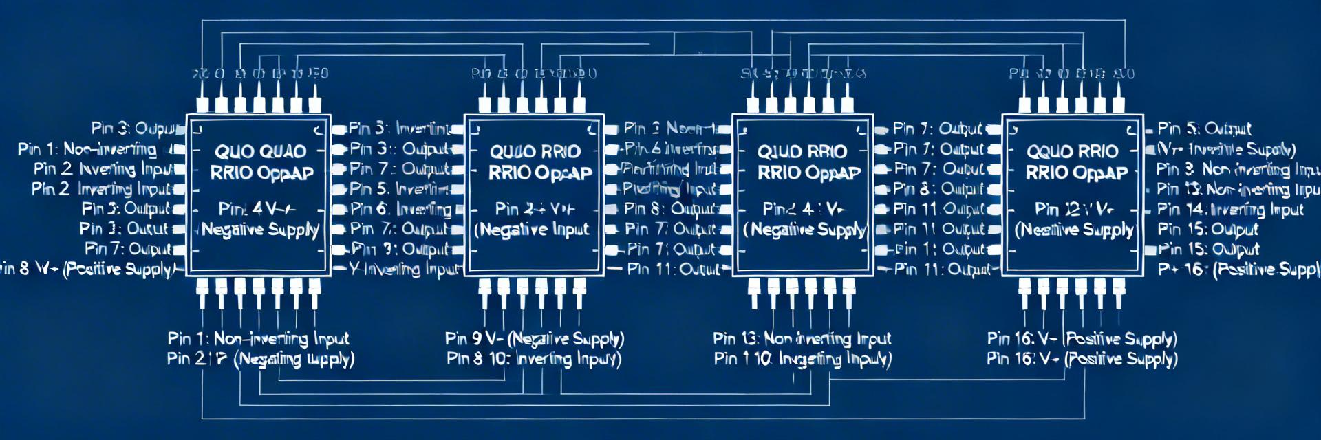
Pinout and Package Configuration
| Pin | Signal | Function |
|---|---|---|
| 1 | OUT1 | Amplifier 1 output |
| 2 | IN−1 | Amplifier 1 inverting input |
| 3 | IN+1 | Amplifier 1 noninverting input |
| V+ | V+ | Positive supply |
| GND | GND | Negative supply / ground |
| Vbypass | Bypass | Internal bias decoupling |
PCB Design Tips
Silk Screening: Use clear silk and power-net naming to avoid misrouting. Group power pins and bypass pins near each other and label nets clearly (VCC, GND, VBIAS).
Thermal Layout: For QFN variants, add thermal vias under the pad. For SOIC, utilize copper pours for heat spreading to ensure long-term reliability.
Design Guidelines & Troubleshooting
Best Practices
- Place 0.1 µF ceramic bypass caps within 2–3 mm of power pins.
- Add a 10–100 Ω series resistor for driving capacitive loads.
- Avoid large input coupling capacitances to prevent phase shift.
Troubleshooting Checklist
- Oscillation? Check bypassing and output isolation.
- Offset Drift? Plan thermal dissipation and check load limits.
- Limited Swing? Verify RL vs datasheet specification.


