
The TPA183A1-S5TR delivers ultra-low input offset in the low tens of µV, selectable fixed gains up to 200 V/V, and a wide common-mode range spanning multiple tens of volts—attributes critical for precision current sensing. This analysis provides an actionable interpretation of the datasheet for practical design applications.
Design Logic & Evidence
Point: Designers require a concise translation of raw metrics into architectural choices.
Evidence: Datasheet parameters define rigorous limits for offset, drift, gain, and Common-Mode Rejection (CMR).
Explanation: The following sections convert these specifications into optimized resistor selections, bandwidth constraints, and deployment checklists for high-reliability production.
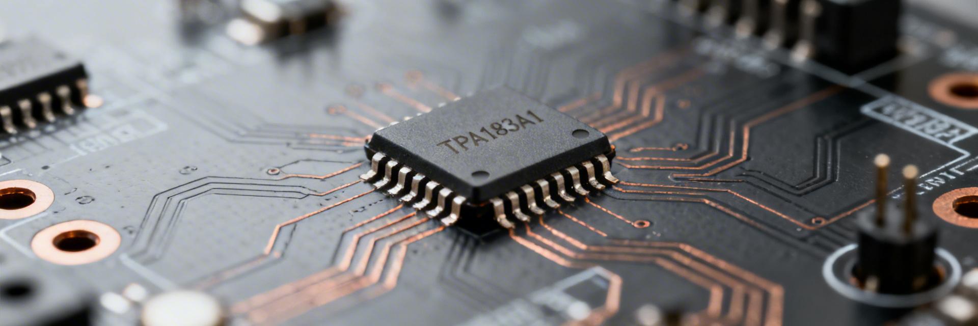
TPA183A1-S5TR: Quick Technical Snapshot
Primary Electrical Highlights
Typical offset of 10–30 µV and drift measured in nV/°C facilitate industry-leading accuracy. Gain options (25, 50, 100, 200 V/V) and high PSRR/CMRR ensure signal integrity across varying bus voltages. Offset, drift, and noise are the dominant factors in precision current-sense resolution.
Package & Absolute Ratings
Housed in a compact SOT-23-5 package, the pinout includes V+, V−/GND, IN+, IN−, and OUT. Absolute maximum ratings for supply and common-mode voltages exceed typical bus levels, offering a safety margin for system integration and rugged environments.
Datasheet Deep Metrics: Electrical Performance & Limits
Gain, Accuracy and Offset Behavior
Fixed gain variants (25/50/100/200 V/V) directly influence effective resolution and dynamic headroom. Designers must utilize "Maximum Error" specifications rather than "Typical" values to ensure production margins, tracking offset drift across the full operating temperature range to maintain ppm-level stability.
Noise, Bandwidth and Dynamic Response
The minimum resolvable current is dictated by the input-referred noise (µV/√Hz) and gain-dependent bandwidth. Selecting the optimal gain involves a trade-off between resolution and the required signal bandwidth for the specific application.
Performance Matrix
| Gain (V/V) | Usable BW (Approx) | Min Resolvable Current* | Visual Bandwidth Scale |
|---|---|---|---|
| 25 | ~1 MHz | ≈100 µA | |
| 50 | ~500 kHz | ≈50 µA | |
| 100 | ~250 kHz | ≈25 µA | |
| 200 | ~125 kHz | ≈12 µA |
*Calculated with a 50 mΩ sense resistor under conservative conditions.
Design & Integration Guidance
Calculation Example
To map a 0–2 A target current to a 3.3 V ADC range using a 100 V/V gain:
Vout = I × Rs × G
Choosing Rs = 10 mΩ yields Vout_max = 2 A × 0.01 Ω × 100 = 2 V.
This provides ample headroom below the 3.3 V rail. A conservative Rs = 8 mΩ is recommended to account for component tolerances.
Protection & Filtering
Implement a small RC filter (10–100 Ω + 10–100 nF) at the inputs to mitigate EMI. In surge-prone environments, utilize TVS diodes or fast-acting fuses. Ensure the input network does not introduce parasitic offsets via bias currents, and decouple the V+ supply immediately adjacent to the package.
Application Scenarios & Comparative Tradeoffs
Battery & Bus Monitoring
Ideal for high-side measurement. Use lower gains (25–50) with larger sense resistors for stable monitoring of discharge rates.
Motor Control
Requires 100–200 gain to capture low-level currents while ensuring the bandwidth is sufficient for high-frequency PWM signals.
Benchmarking Checklist
Prioritize offset & drift for precision. Penalize parts with insufficient bandwidth at target gain. Factor in thermal limits for high-density layouts.
Practical Test & Deployment Checklist
- ✓ Lab Verification: Measure DC offset with shorted inputs and verify gain accuracy using a precision current source.
- ✓ Dynamic Stress: Perform temperature sweeps in a thermal chamber to correlate drift with datasheet specifications.
- ✓ Troubleshooting: Check for saturation signatures by auditing output headroom and supply rail stability under load.
Summary & Key Takeaways
The TPA183A1-S5TR is a robust solution for precision current sensing, combining ultra-low offset with versatile gain options. Effective implementation relies on balancing resolution against bandwidth and maintaining rigorous safety margins against datasheet maximums.
- Select gain to optimize SNR; higher gain improves resolution but narrows the usable frequency response.
- Always design based on maximum offset and drift values to ensure reliability across mass production.
- Validate performance through DC offset, gain calibration, and thermal testing before final deployment.


