
Background & Quick-Spec Snapshot
Datasheet Highlights — What to Extract First
First pull: supply range (2.5–6 V), typical quiescent current (~600 μA/channel), unity-gain bandwidth (~6 MHz), rail-to-rail input/output behavior, recommended load and output swing limits. Next, note input common-mode window and offset characteristics; these determine headroom and accuracy in single-supply sensor front ends and low-voltage ADC drivers.
Typical Application Scenarios and Fit
Best fits are portable analog front-ends, low-power sensor interfaces, and signal conditioning where battery operation and rail-to-rail swing matter more than very high bandwidth. Designers trade off the modest 6 MHz bandwidth and mid-uA bias current for simplicity and single-supply operation; choose alternatives if high-drive current or multi-MHz large-signal slew is required.
Electrical Performance Deep-Dive
Input/Output Behavior, Noise, and Frequency Response
Interpret input offset as the DC error budget; combine offset, bias, and ADC quantization when budgeting system accuracy. Check input common-mode limits to ensure signals remain in the linear region. For frequency response, plot gain vs. frequency and compare measured –3 dB point to the datasheet GBW; perform a noise spectrum sweep to validate noise density against application SNR requirements.
Power, Temperature, and Stability Considerations
Characterize quiescent current across the supply and operating temperature range to size batteries and thermal margins. Verify thermal derating if the package dissipates multiple channels. Confirm unity-gain stability and recommended load capacitance limits; add small series resistances in the feedback path if capacitive loads cause ringing or oscillation.
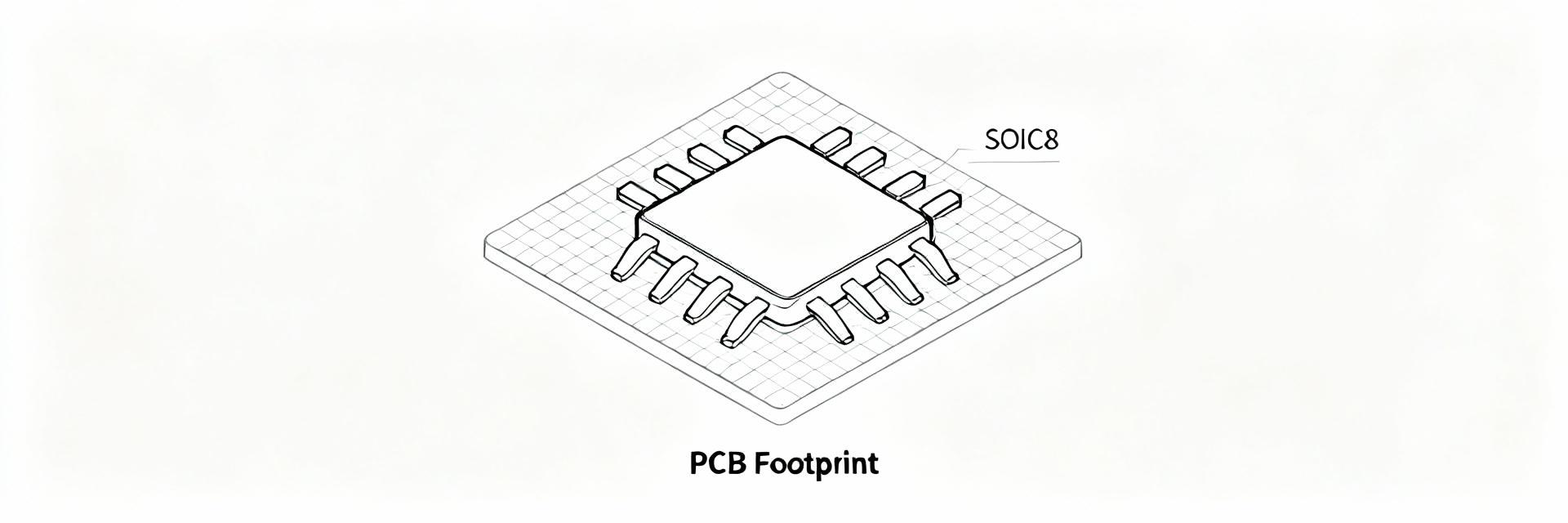
SOIC8 Footprint & Land-Pattern Specifics
Recommended Land Pattern
Use an IPC-consistent SOIC8 land pattern: pitch 1.27 mm, pad length 1.5 mm, pad width 0.45 mm, toe-to-toe spacing per body width. Keep solder mask defined between pads, maintain a 0.25–0.5 mm keepout around the package body for assembly tolerances, and avoid placing vias inside pads.
| Feature | Recommended |
|---|---|
| Pad Pitch | 1.27 mm |
| Pad Length (L) | 1.50 mm ±0.05 |
| Pad Width (W) | 0.45 mm ±0.05 |
| Body Dim. | ~5.0 mm × 3.9 mm |
Solder & 3D Model Tips
Use 60–70% paste coverage per pad as a starting point (aperture area / pad area) to balance wetting and tombstoning risk. For long pads prefer segmented apertures or 3:1 ratio length-to-width to improve paste release. Add a 3D STEP model to the library for collision checks; inspect lead coplanarity risk during pick-and-place programming.
PCB Layout Best Practices & EMI/Thermal Tips
Stability & Grounding
- Place 0.1 μF decoupling within 1–2 mm of VCC.
- Add 1 μF bulk for load transients.
- Keep input traces short; use single-point feedback.
- Stitch ground planes to reduce loop area.
Thermal & EMI
- Use copper pours for heat spreading.
- Implement guard traces for sensitive inputs.
- Keep noisy digital returns on separate planes.
- Run quasi-static EMI checks before fabrication.
Prototype Testing & Assembly
Bench Test Checklist
Follow a step sequence: verify power rails and quiescent current, measure input offset and low-frequency gain, run a small-signal gain vs. frequency sweep to confirm –3 dB point, measure output swing under expected load, and perform a noise spectral density capture. Use short leads, proper shielding, and reference the Datasheet test conditions when comparing results.
Reflow & Production
Adopt a ramp-to-peak reflow profile consistent with the SOIC8 thermal mass. Ensure board fiducials are present, clean pads before placement, and inspect solder fillets, coplanarity, and voiding via X-ray for qualification lots. Validate part marking against the supplier label to ensure correct device revision and traceability.
Summary
- ★ Key Datasheet Checks: Verify supply range (2.5–6 V), quiescent current (~600 μA/channel), GBW (~6 MHz), and rail-to-rail I/O before layout.
- ★ Footprint Decisions: Use 1.27 mm pitch, 1.5 mm pad length, and 60–70% stencil aperture to minimize tombstoning risks.
- ★ Layout & Test: Maintain tight decoupling, minimize feedback loops, and follow a systematic bench checklist to catch DC/AC issues early.
Frequently Asked Questions
What key Datasheet values should be validated on bench for TP1562AL1-SO1R-S?
How should the SOIC8 footprint be adjusted to avoid tombstoning?
What are first-pass production inspection priorities for this SOIC8 device?


