
Point: The article targets repeatable measurement and design decisions.
Evidence: It bundles absolute limits, recommended operating ranges, thermal guidance, dynamic curves to capture (GBW, slew, noise), and repeatable fixture practices into a single reference.
Explanation: Readers gain a reproducible test plan and interpretation guide that reduces debug cycles and lets teams validate device behavior against the electrical specs expected in portable signal‑conditioning and buffer applications.
Product Overview & Key Specs
At-a-glance Spec Snapshot
| Parameter | Typical / Min / Max | Notes |
|---|---|---|
| Supply Voltage (Vcc) | 2.5 V — 6.0 V (recommended) | Defines allowable headroom for rails and bias networks |
| Supply Current (per channel) | ~600 µA typical | Budget for quiescent power in multi‑channel systems |
| Output Drive | ±10–20 mA range | Specifies short‑term load capability and drop under DC load |
| Bandwidth (small‑signal) | ~6 MHz (unity/Gain‑BW region) | Determines closed‑loop bandwidth limits for filters/amplifiers |
| Input/Output Common‑Mode | Rail‑to‑rail claimed | Impacts sensor interface range and signal swing |
| Operating Temp | Industrial range typical | Important for drift and derating calculations |
| Package | SOIC / SO variants | Influences thermal resistance and PCB layout |
Point: Each table row maps to practical design checks.
Evidence: Supply limits set headroom; I/O common‑mode and bandwidth determine whether the device suits low‑voltage portable instrumentation.
Explanation: Use the table as a quick acceptance checklist: if nominal system rails, required bandwidth, and load current match the rows, proceed to lab validation; otherwise re‑evaluate architecture or select buffering stages.
Typical Use Cases and Limitations
Point: Typical application classes are low‑voltage signal conditioning, portable instrumentation, and buffer stages.
Evidence: The combination of low quiescent current and rail‑to‑rail I/O suits battery‑powered front ends and ADC drivers.
Explanation: Limitations include that the device is not intended for high‑speed RF or heavy capacitive drive; designers should avoid driving large capacitive loads directly and should not expect high output current for power‑stage tasks.
Electrical Ratings & Operating Conditions
Absolute Maximums and Recommended Operating Range
Point: Absolute maximums differ from recommended operating ranges; stay within recommended ranges for reliability.
Evidence: If absolute VCC abs max is >6 V, designers normally derate to 90–95% of that value at elevated temperatures.
Explanation: Example: with recommended Vcc max = 6.0 V and an absolute max ~7.0 V, target system rail ≤6.0 V and apply derating at high Ta; maintain margin so transient spikes and ESD events do not exceed abs limits.
Thermal and Supply Considerations
Point: Power dissipation drives junction temperature and limits sustained output.
Evidence: Estimate Pd ≈ Icc_total × Vcc + (Iout_avg × Vdrop) for loaded conditions; package θJA and ambient determine ΔT.
Explanation: Sample calc: with two channels at 600 µA each on 5 V, Icc_total = 1.2 mA → Pd ≈ 6 mW base. Add dynamic dissipation under load.
Visualized Power Calculation (Pd)
Dynamic Performance: Frequency, Slew, Noise
Small-signal Response & Bandwidth
Point: Capture gain‑bandwidth and open‑loop gain vs frequency to predict closed‑loop behavior.
Evidence: Test at Vs = nominal Vcc, RL = typical load (10 kΩ), input amplitude small (tens of mV).
Explanation: Recommended caption: “Small‑signal gain vs frequency (Vs = 5 V, RL = 10 kΩ)”; expect a single‑pole rolloff into GBW near the 6 MHz region and monitor phase to infer stability margins.
Slew Rate, Settling Time & Noise
Point: Slew and settling define transient fidelity; input‑referred noise sets resolution floor.
Evidence: Measure slew with a step input; measure noise density with a low‑noise preamp and integrate over 0.1 Hz–10 kHz.
Explanation: Document test bandwidths; report slew in V/µs, 0.1–10 kHz integrated noise in nV/√Hz integrated to µV RMS.
DC Performance: Offsets, Bias, PSRR/CMRR
Input Offset, Drift and Bias Current
Point: Measure Vio, drift, and input bias to judge accuracy.
Evidence: Use a precision DVM, thermally stabilize the DUT, sweep Ta across operating range and record Vio at multiple temps.
Explanation: Provide a simple table for recording Vio (typ/max) at 25°C, −40°C, and +85°C to estimate error contributions in high‑impedance sensor chains.
Power-supply Rejection & Common-mode Rejection
Point: PSRR and CMRR quantify immunity to supply and common‑mode perturbations.
Evidence: Modulate supply with known AC amplitude (e.g., 100 mV peak at 1 kHz); for CMRR apply common‑mode AC while differential inputs are zero.
Explanation: Plot PSRR/CMRR vs frequency (log scale) and report amplitude in dB; include frequency points at 10 Hz, 1 kHz, 10 kHz.
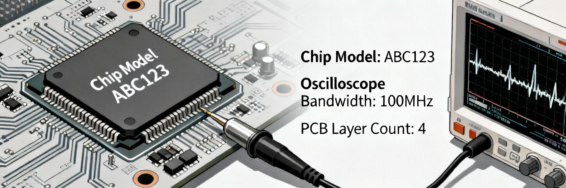
Test Setup, Fixtures & Measurement Best Practices
Recommended Test Rig and Instruments
Point: Proper instruments and grounding reduce measurement error.
- Low‑noise supply, 0.1% regulation
- Waveform generator with fast edges
- Oscilloscope ≥100 MHz with active probes
- Network or FFT analyzer for PSRR/noise
- Programmable load or precision resistor bank
Explanation: Pre‑test checklist: verify supply decoupling close to device pins, short scope ground leads, and a PCB layout with solid ground return.
Repeatable Procedures & Data Logging
Point: Procedural consistency ensures comparable datasets.
Evidence: Execute DC, AC, and transient tests in a defined sequence and record meta tags.
Explanation: Recommended CSV columns: test_id, Vs, RL, Ta, Vio, Icc, GBW, slew, noise_rms, fixture_id, date. Run multiple samples (n≥5) for statistics.
Sample Measured Data, Example Plots & Application Notes
Example Measured Tables and Annotated Plots
Point: Prioritize a core set of plots and tables for validation.
Evidence: Include summary spec table, gain vs frequency, THD vs output amplitude, output swing vs load, supply current vs Vs, offset vs temperature, and slew/settling plots.
Explanation: For each plot indicate axes and conditions in captions (e.g., “Output swing vs RL (Vs = 5 V): X‑axis = load, Y‑axis = peak output swing”) and add a short interpretation line describing pass/fail cues.
Practical Design Checklist & Troubleshooting Tips
Point: A condensed checklist and fast troubleshooting flow speeds problem solving.
Checklist Items
- Decoupling caps (0.1 µF + 10 µF)
- Input protection diodes for overdrive
- 25–100 Ω series output resistor for capacitive loads
- Thermal vias near package
Troubleshooting Flow
Symptom → Likely Cause → Corrective Action
Example: Oscillation → Insufficient damping → Add series resistor.
Summary
Point: This technical dossier aggregates the key testable attributes and practical guidance for evaluation.
Evidence: It emphasizes the TP1562AL1-SO1R-S headline numbers and maps test methods to measurable outcomes while referencing the manufacturer datasheet for full parameter definitions.
Explanation: Main takeaways: validate supply and thermal margins first, capture small‑signal and transient curves under representative loads, and log structured CSV data for statistical confidence; these steps ensure measured performance aligns with electrical specs required for robust designs.
Key Summary
- TP1562AL1-SO1R-S fits low‑voltage portable signal conditioning: verify rails (2.5–6 V), Icc ~600 µA/channel, and GBW ≈6 MHz before layout commitment.
- Measure thermal dissipation using Pd ≈ Icc_total×Vcc and confirm junction rise via θJA; derate supply at high ambient to protect margins.
- Capture GBW, slew, settling, PSRR, and noise with defined captions and test conditions; integrate noise over the target bandwidth for meaningful RMS figures.
Frequently Asked Questions
How should TP1562AL1-SO1R-S be powered and decoupled for best results?
What test sequence yields reproducible electrical specs for TP1562AL1-SO1R-S?
What are common fixes if the device oscillates during testing?


