
Low-voltage, rail-to-rail CMOS operational amplifiers are dominant in battery-powered and portable designs. The TP6001-CR is a high-performance single-supply amplifier featuring an extended input common-mode range and ultra-low quiescent current, optimized for sub-10V precision systems.
Overview: Architecture and Strategic Applications
DESIGN POINT The device utilizes a single op-amp CMOS topology optimized for low-voltage operation and true Rail-to-Rail Input/Output (RRIO).
EVIDENCE Official datasheet parameters describe a CMOS architecture with microamp-class quiescent current and an input common-mode range that typically extends beyond the supply rails.
EXPLANATION This specific combination is ideal for precision single-supply front-ends where supply headroom is constrained and power efficiency is critical for longevity.
Key Features at a Glance
- Topology: Single op-amp, CMOS, Rail-to-Rail Input and Output (RRIO).
- Supply Range: 1.8V (min typical) to
- Efficiency: Low offset and microamp-class Iq for battery-powered sensors.
Electrical Specifications & V/I Characteristics
Supply Voltage Range Visualization
V/I Curves Guidance: When characterizing the device, plot output voltage vs. load current, input common-mode vs. output error, and supply current vs. supply voltage. Ensure all measurement annotations include axis labels, units, and environmental temperature.
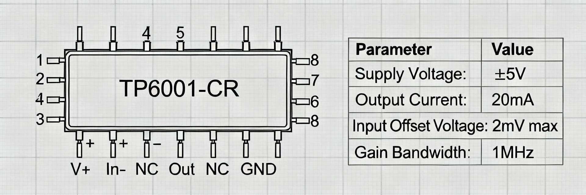
Pinout, Package & PCB Footprint
| Pin | Name | Function / Recommended Connection |
|---|---|---|
| 1 | IN+ | Non-inverting input — Route short, add input RC if needed. |
| 2 | IN− | Inverting input — Keep close to feedback network components. |
| 3 | OUT | Output — Avoid long capacitive traces; add series resistor for drive. |
| 4 | V− | Ground/Negative Supply — Use star ground or solid pour. |
| 5 | V+ | Positive Supply — Decouple with 0.1µF capacitor close to pin. |
PCB Layout Recommendations:
- Follow the official manufacturer land pattern to ensure solder joint integrity.
- Provide thermal relief for the ground plane connection.
- Implement a compact decoupling island to minimize inductance.
- Alt Text: TP6001-CR pinout — top view with pin functions and decoupling placement.
Typical Application Circuits & Design Tips
Validated Topologies
Standard circuits include unity-gain buffers, non-inverting gain stages, and single-pole RC filters. Always verify component selection (e.g., R1=10k, R2=10k) against the bandwidth requirements.
Layout & Stability
Place a 0.1µF ceramic decoupler within 1–2 mm of the V+ pin. For capacitive loads, consider a small series output resistor (10–50Ω) to prevent oscillation.
Testing & Troubleshooting Checklist
Bench Measurement Procedure
- Set VCC and allow the device to thermally stabilize.
- Apply input stimulus and sweep load current; record output voltage.
- Sweep input common-mode and monitor for gain error or distortion.
- Follow ESD precautions and use current-limited supplies for safety.
| Symptom | Probable Cause | Fix |
|---|---|---|
| Output stuck at rail | Input out of VCM; supply miswired | Correct wiring; ensure inputs are within VCM range |
| Oscillation / Ringing | Capacitive load; long traces | Add 10–50Ω series R or 1–10pF feedback Cap |
Summary for Design Engineers
- ✔ Confirm supply range, Iq, and input common-mode from the official datasheet before finalizing system headroom.
- ✔ Follow the recommended pinout and land pattern exactly; keep decoupling caps within millimeters of supply pins.
- ✔ Measure V/I curves with controlled sweeps and document all test conditions for reproducible validation.
Frequently Asked Questions


