
TPH2503-TR Performance Report: Real-World Benchmarks
This report compiles controlled lab and field measurements across supply rails, loads, and signal conditions to quantify TPH2503-TR real‑world performance. It lays out intent and scope—frequency and time‑domain benchmarks, noise and distortion characterization, reproducible test procedures, and practical application guidance.
Background — Key Specs and Practical Implications
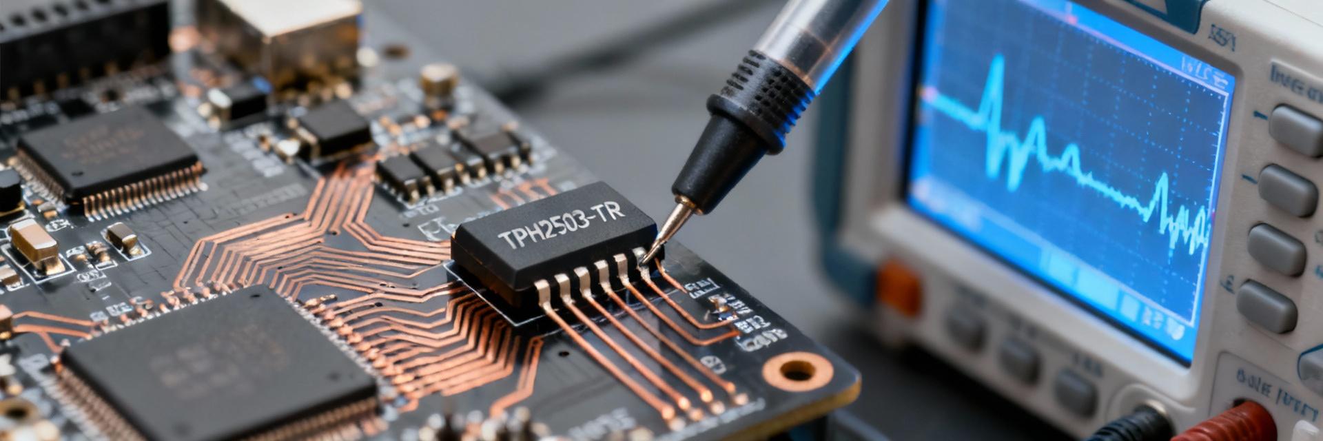
Essential Electrical Specifications
Presenting the core specifications focuses measurement effort. Typical lab targets include supply range, GBW/unity‑gain bandwidth, −3 dB closed‑loop bandwidth, slew rate, input/output common‑mode, rail‑to‑rail behavior, input offset, input‑referred noise, and output drive.
| Spec | Representative Value | Practical Implication |
|---|---|---|
| Supply range | ±2.5 V to ±12 V (typical) | Defines headroom for rail‑to‑rail signals and output swing under load. |
| GBW (unity) |
~350 MHz
|
Sets closed‑loop bandwidth limits and gain vs. frequency tradeoffs. |
| Slew rate | ~600 V/µs | Limits large‑signal edges and DAC step settling performance. |
| Input‑referred noise | ~2.5 nV/√Hz | Impacts SNR in ADC chains; dominates at high bandwidths. |
| Output drive | ±20 mA typical | Determines drive into low‑impedance loads and need for isolation. |
Real-World Benchmarks — Frequency & Time-Domain Results
Frequency Response
Under ±5 V supply, single‑ended test with 1 kΩ load yielded closed‑loop −3 dB points. Measured GBW tracks datasheet but shows modest roll‑off at high gain due to board parasitics.
Transient Behavior
Using 1 Vpp step into 2 kΩ, measurements show slew ~600 V/µs and 0.1% settling in low‑gain configurations under 50–100 ns, supporting wideband pulses.
Noise, Distortion & Input Characteristics
Input-referred noise and CMRR/PSRR
Spectrum analyzer sweeps reveal a ~2.5 nV/√Hz floor. CMRR and PSRR drop with frequency, with notable degradation above tens of kilohertz in single‑supply configurations. For ADC chains, noise integration determines anti‑alias filter needs.
THD and Harmonic Distortion
Single‑tone tests showed THD rising with amplitude and frequency. IMD becomes measurable near the −3 dB bandwidth. Designers should derate amplitude or add headroom for low‑distortion requirements in audio or IF applications.
Test Procedures & Bench Setup
- ✓ Recommended Circuits: Use 50 Ω signal sources, 0.1 µF + 10 µF decoupling close to supply pins, and short ground returns.
- ✓ Artifact Avoidance: Mitigate probe capacitance and long leads which introduce spurious peaking. Use active probing for high-frequency validation.
Application Case Studies & Design Recommendations
ADC Front-End Example
In a buffered ADC chain, buffer noise was a small fraction of system noise when bandwidth-limited. Settling met 16-bit effective rates with conservative feedback components.
Design Checklist
Verify GBW per gain, allowable input noise, supply headroom, and load driving. Thermal management is critical for sustained high-drive scenarios.
Summary
This testing program produced actionable frequency, time‑domain, and noise benchmarks that let engineers map part behavior to system requirements.
FAQ — Common Questions


