Core Insight: The TP2121 occupies the nanowatt-class niche, with per-amplifier supply current specified around 600 nA typical and up to 950 nA max.
Objective: This analysis translates datasheet metrics into concrete design decisions for low-power analog front ends.
Background: What the TP2121 Is and Where It Fits
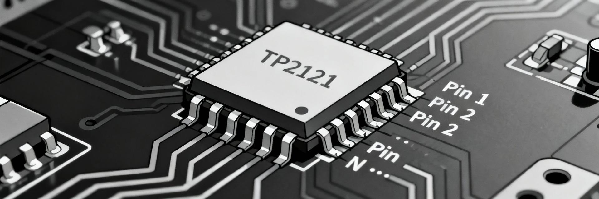
Product Class & Core Strengths
The TP2121 is an ultra-low-power CMOS precision operational amplifier designed for always-on sensor interfaces. Its nanowatt-class quiescent current and rail-to-rail behavior make it ideal for battery-powered temperature or strain sensors.
Typical Operating Conditions
Specified across a wide low-voltage supply window, it supports single-cell battery operation while preserving input common-mode and output swing margins for maximum signal integrity.
Key Electrical Specs: Interpreting the Numbers
| Parameter | Typical / Target | Design Note & Visualization |
|---|---|---|
| Supply Current | ~600 nA / 950 nA max |
Power Budgeting
|
| GBWP | ~18 kHz |
DC to low-kHz filters
|
| Slew Rate | ~10 mV/µs | Limits fast transient response |
| Offset Voltage | Sub-mV | Precision signal conditioning |
Dynamic Performance Note: High closed-loop gains reduce usable bandwidth. Pick gains so the closed-loop bandwidth remains well below GBWP/G to maintain stability margins.
Pinout & Electrical Mapping
- Functional Map: Includes V+, V-/GND, Non-inverting/Inverting inputs, and Output.
- ESD Protection: Plan for ESD diodes or series resistors at inputs when exposed.
- Signal Limits: Ensure sensor signals remain inside the common-mode window to avoid rail saturation.
PCB Layout Best Practices
- Grounding: Use a solid ground plane to minimize noise and stability issues.
- Bypassing: Place a 0.1 µF bypass capacitor within 1–2 mm of the V+ pin.
- Routing: Route input traces short and shielded to avoid star routing return paths.
Application Examples & Configurations
Low-Power Sensor Front End
Typical single-supply sensor amplifier uses R values (100 kΩ–1 MΩ) to keep input bias currents negligible. Recommended gain of 10–50 for DC-oriented sensors.
Energy-Harvested Monitor
Configured as a comparator with hysteresis to conserve power. Feedback networks should be high-value to minimize current consumption during threshold detection.
Troubleshooting & Validation Checklist
- Instability (ringing/oscillation)
- Unexpected DC offset drift
- Excessive current draw near rails
- Low-noise power supply
- Short grounding probe tips
- AC small-signal sweep for GBWP
Frequently Asked Questions
What supply voltages are recommended for the TP2121?
How should I interpret the TP2121 pinout in schematics?
What are quick lab checks to verify datasheet specs?
