
Focuses on DC/AC parameters, pinout configurations, and thermal limits to streamline schematic capture and PCB bring-up.
Quick Background: What the TP6004-SR is and When to Pick It
Device Family Snapshot
Point: CMOS single-supply operational amplifier class optimized for low supply voltages and low idle current.
Evidence: Operation below 5V with RRIO outputs and low offset figures.
Explanation: Ideal for sensor front-ends and portable instrumentation where precision meets long battery life.
Selection Criteria Checklist
- ✓ Gain-Bandwidth Product (GBW)
- ✓ Slew Rate & Output Drive
- ✓ Input Offset & Common-mode Range
Electrical Specs Deep-Dive
| Parameter Type | Key Metrics | Design Consideration |
|---|---|---|
| Static / DC Specs | Vos, Iq (~80 μA), CMRR, PSRR | Derate offset/bias for worst-case temperature. |
| Dynamic / AC Specs | GBW (~1 MHz), Slew Rate, Phase Margin | Set -3 dB BW ≈ GBW/Closed-loop gain. |
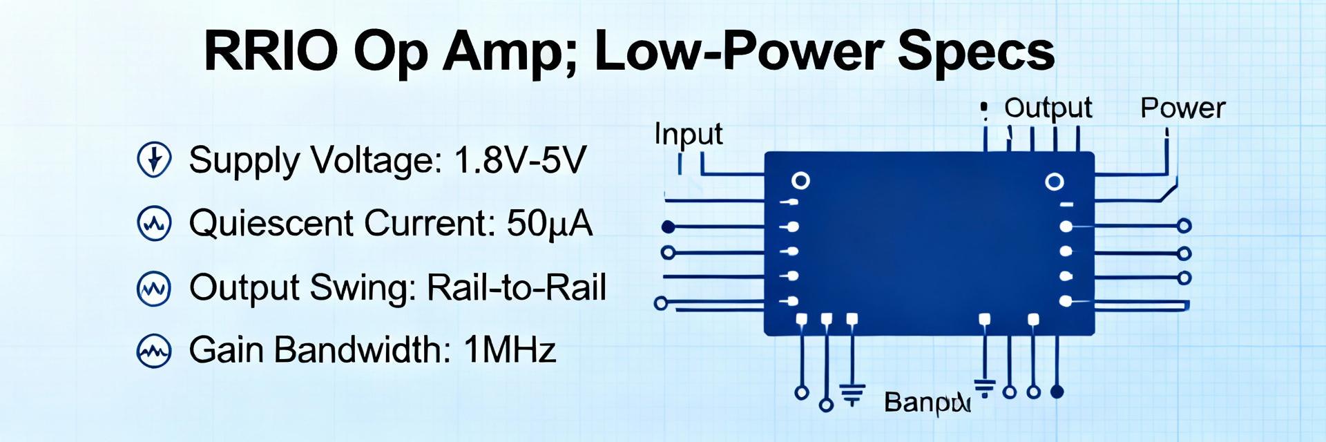
Pinout & Package Details
Electrical Pin Notes
Typical configuration includes V+, V-/GND, +IN, -IN, and OUT. Ensure input protection diodes are considered and avoid floating pins to maintain stability.
Footprint Guidance
Commonly available in SOT-23 and SOIC/SOP. Keep analog ground returns short and use thermal vias if high dissipation is expected.
Absolute Limits & Constraints
Typical Performance & Bench Verification
Reading Curves
Watch for test conditions on PSRR and Open-loop gain plots. Output swing specs at light loads will not hold under heavy resistive loads.
Recommended Tests
Verify DC offset, unity-gain stability, and slew rate. Use proper bypassing and short probe grounds to avoid induced ringing.
Integration & Troubleshooting
PCB Checklist
- Supply decoupling (0.1μF + 1μF) close to pins.
- Series resistors for input protection.
- Separate analog and digital return paths.
Debugging Steps
- Oscillation? Check decoupling/output capacitive load.
- Limited swing? Check supply rails and load impedance.
- High offset? Inspect for ESD or leakage paths.
Summary & Key Takeaways
The TP6004-SR concept targets low-voltage, low-power RRIO amplifier use in battery and sensor applications, emphasizing μA-class quiescent current and modest GBW.
Common Questions and Answers


