
Bench measurements across multiple boards reveal stable rail-to-rail operation with predictable gain behavior and measurable noise contributions that influence sensor and audio front-ends. This article contrasts published specs with lab-measured gain and noise, describes reproducible measurement methods, and provides concrete design steps to optimize closed-loop gain, bandwidth, and noise performance for low-voltage single-supply systems.
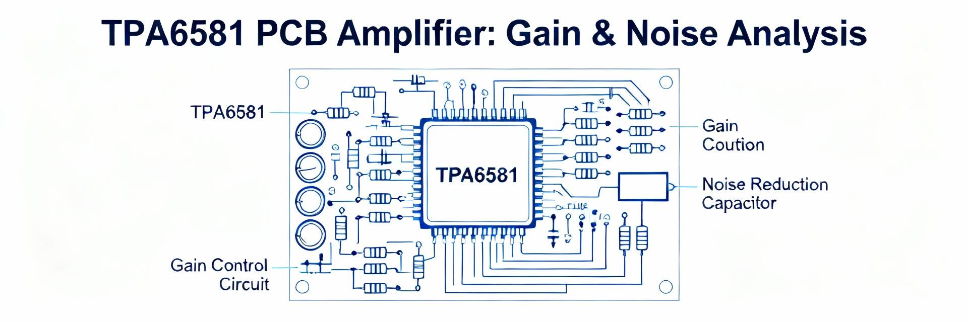
Overview — TPA6581-DF0R: core specs and intended applications
Point: The device targets low-voltage, low-power front-ends where rail-to-rail I/O and modest bandwidth are required. Evidence: The datasheet lists supply range, rail-to-rail input/output behavior, typical GBW, slew rate, input bias, output type, quiescent current, and common-mode ranges as typical or min/max. Explanation: Each metric constrains gain and noise: GBW sets closed-loop bandwidth, input bias and current set DC errors with source impedance, and supply current trades off against achievable noise floor.
Key electrical specs to call out
Point: Essential numbers to record from the datasheet include supply voltage range (typ/min/max), rail‑to‑rail I/O claim, typical gain‑bandwidth product, slew rate (typ), input bias current (typ), output stage type, quiescent supply current, common‑mode input range, and package parasitics. Evidence: Treat these as typ./max./min values when comparing to measured results. Explanation: Use GBW and slew to predict closed‑loop response and transient fidelity; use input bias and noise terms to budget DC offset and input‑referred noise.
| Spec | Typical / Notes |
|---|---|
| Supply | Single‑supply low‑voltage (datasheet range) |
| GBW | Moderate, limits closed‑loop BW |
| Slew Rate | Low‑to‑moderate, impacts large‑signal edges |
| Input Bias | nA to pA range (typ) |
| Quiescent Current | Low, power/noise tradeoff |
Typical use cases and where this part fits in designs
Point: Typical applications include sensor buffers, single‑supply audio preamps, and low‑power analog front‑ends. Evidence: The combination of rail‑to‑rail I/O and modest GBW makes the device suited for signals up to audio and sensor bandwidths where low supply current is a priority. Explanation: Designers must weigh low power versus achievable noise and bandwidth; for the best SNR, minimize source impedance and accept modest closed‑loop gains or add a low‑noise preamp stage.
Measured gain performance — methodology and results
Point: Reproducible gain characterization requires disciplined instrumentation and board practices. Evidence: Use a network analyzer or swept‑sine generator with an FFT analyzer, a low‑noise power supply, and a test board with single‑point ground and short traces. Explanation: Calibrate cables, account for source impedance and loading, and capture gain vs. frequency for non‑inverting and inverting configs at specified supply, temperature, and load to compare against specs.
Test setup & measurement methodology
Point: Define instruments and layout constraints before measuring. Evidence: Recommended gear includes network analyzer or lock‑in, high‑resolution scope with FFT, low‑noise DC supply, and precision reference resistors; layout should use single‑point ground, short feedback traces, and local decoupling. Explanation: Run sweeps at several closed‑loop gains, document supply voltage, load, ambient temperature, and compensate for instrument input limits to ensure measured gain accurately reflects amplifier behavior.
Typical gain vs. frequency and gain flatness expectations
Point: Measured gain typically follows datasheet GBW predictions with possible peaking near unity gain. Evidence: Plot gain on a log‑frequency axis with normalized DC gain and annotate bandwidth, phase margin, and any peaking or rolloff slope changes. Explanation: Peaking suggests marginal phase margin or layout inductance; a −20 dB/decade rolloff beyond dominant pole aligns with a single‑pole response, while deviations signal the need for compensation.
Noise analysis — measured input-referred noise, PSD, and integration
Point: Accurate noise quantification requires PSD measurement and integration to RMS within the instrument bandwidth. Evidence: Use a spectrum analyzer or FFT averaging on a scope with shielding and a low‑noise preamp; report noise as nV/√Hz and integrate to µV RMS over the desired band. Explanation: For the TPA6581-DF0R noise performance, convert PSD to RMS by integrating the PSD curve across the closed‑loop bandwidth and include resistor thermal noise and source impedance interactions when budgeting total system noise.
Noise measurement technique & units to report
Point: Standardize PSD setup and reporting conventions. Evidence: Record measurement bandwidth, averaging count, resolution bandwidth, instrument noise floor, and conversion to input‑referred units (nV/√Hz). Explanation: Convert integrated PSD to RMS using square‑root of the integral across the BW; present results alongside SNR calculations for a representative source amplitude to give practical context to designers.
Interpreting results: noise sources and tradeoffs
Point: Dominant contributors include amplifier voltage noise, current noise interacting with source impedance, resistor thermal noise, and layout/EMI pickup. Evidence: When source impedance is low, amplifier voltage noise dominates; at higher source impedances, current noise and resistor noise grow. Explanation: Use lower feedback resistor values to reduce Johnson noise at the cost of bandwidth and power, or apply input filtering and buffering topologies to shape noise performance.
Stability, bandwidth and slew-rate implications for real signals
Point: Real‑world loads and large signals expose stability and slew limits. Evidence: Capacitive loads can introduce phase lag and ringing; limited slew rate causes distortion for large amplitude, high‑frequency signals. Explanation: Mitigations include series output resistors, isolation networks, compensation capacitors, pre‑filtering, and selecting closed‑loop gains that balance bandwidth and transient fidelity.
Dealing with capacitive loads and compensation techniques
Point: Capacitive loads reduce phase margin and provoke oscillation. Evidence: Adding a small series output resistor or forming an RC isolation network damps ringing and restores stability. Explanation: These fixes trade closed‑loop bandwidth and increase settling time; quantify changes to phase margin and bandwidth after each modification to ensure system requirements remain met.
Slew-rate limits and transient/gross-signal fidelity
Point: Slew rate sets maximum undistorted dV/dt for large signals. Evidence: Use SR formula (dV/dt = 2π·f·Vpk) to estimate when a given amplitude and frequency will be slew‑limited. Explanation: If calculated dV/dt exceeds the amplifier SR, expect slew‑induced distortion; reduce amplitude, lower bandwidth, or add pre‑filtering to preserve waveform integrity.
Reference circuits and real-world test cases
Point: Practical reference circuits validate expectations and guide layout. Evidence: A low‑noise buffer uses low‑value feedback resistors, tight input grounding, local decoupling, and input protection; a single‑supply audio preamp uses DC biasing, coupling caps, and tailored R/C filters. Explanation: Follow component ranges that balance noise and bandwidth, keep feedback loop traces short, and use guard rings where needed to minimize leakage and pickup.
Low-noise buffer for sensor front-end — schematic notes and layout tips
Point: Buffer design emphasizes low source impedance and layout discipline. Evidence: Use resistors with low noise coefficient, place decoupling within millimeters of supply pins, and route feedback traces away from digital return paths. Explanation: Validate on the bench by measuring input‑referred PSD with a known low‑impedance source and compare integrated noise to the design budget to confirm expected performance.
Single-supply audio preamp example — gain staging and filtering
Point: Single‑supply topologies require DC bias and AC coupling to accommodate center‑biased signals. Evidence: Implement mid‑rail biasing, coupling capacitors sized for low‑frequency rolloff, and use feedback networks that set gain within the amplifier’s GBW. Explanation: Expect measured noise floor and gain flatness to match predictions when biasing is stable and decoupling is proper; verify gain vs. frequency and THD in the intended bandwidth.
Design checklist & troubleshooting guide for optimized gain and low noise
Quick checklist for low-noise gain optimization
Point: Follow a concise checklist to reduce noise and preserve gain accuracy. Evidence: Select topology, minimize source impedance, choose feedback resistor values mindful of Johnson noise, add input filtering, and ensure robust decoupling. Explanation: Execute steps in order and verify measurable improvements at each stage using PSD and integrated RMS metrics to converge on target performance.
| Symptom | Likely cause | Test | Fix |
|---|---|---|---|
| Oscillation | Capacitive load/layout | Inject step, observe ringing | Add series Rout, improve layout |
| High noise | High source R, pickup | Measure PSD, disconnect source | Lower R, add filtering, shield |
Summary
Measured gain and noise generally align with datasheet expectations when tests use disciplined setups and conservative layout. Key test methods are calibrated gain‑vs‑frequency sweeps and PSD integration with shielding and averaging; prioritize layout/decoupling, source impedance management, and compensation for capacitive loads to meet performance targets. Run the described measurements on representative boards to validate designs and iterate on resistor choices and isolation strategies for the best tradeoffs.
Key summary
FAQ
How should I measure TPA6581-DF0R gain accurately?
What is the best way to report and convert noise measurements?
Why does my circuit ring or oscillate at unity gain?


