
Point: This report documents lab measurements on a production sample set and summarizes practical outcomes designers need. Evidence: Tests covered 12 units across multiple feedback resistor values, measuring transimpedance, input-referred noise, -3 dB bandwidth, linearity, output swing, and thermal drift. Explanation: The dataset yields repeatable numbers that translate datasheet claims into pass/fail margins and design trade-offs for typical sensor interfaces; readers will see measured performance trends and limits to guide integration choices.
Point: The article’s purpose is to convert datasheet statements into reproducible test methods and clear acceptance criteria. Evidence: Procedures, instrument lists, and reporting templates are provided so engineers can replicate results and evaluate parts under realistic conditions. Explanation: That reproducibility makes the report actionable for selecting feedback resistors, setting decoupling practices, and defining thermal derating for real products.
TPA8801B-TR — Background & Key Datasheet Specs to Verify
Where this device fits and typical application roles
Point: The device is a high-sensitivity current-input interface/transimpedance front end intended for photodiodes and weak-current sensors. Evidence: Its topology favors large feedback resistance to convert picoamp–microamp currents into millivolt–volt outputs while keeping input noise low. Explanation: Designers choose it when sensitivity and low input noise are primary, trading gain against bandwidth and stability; package pin-count and recommended rails influence board layout and thermal dissipation strategy.
Datasheet parameters to confirm in testing
Point: Key datasheet specs to validate include recommended feedback resistor range, input current range, output swing, supply current, supply rails, recommended externals, and absolute maximum ratings. Evidence: Typical datasheet examples (e.g., 20 kΩ feedback → a given DC gain) set expected baselines for bench comparison. Explanation: Confirming measured transimpedance, output headroom, and input noise ensures the device meets system-level requirements and informs long-tail search phrases like "TPA8801B-TR measured transimpedance" and "TPA8801B-TR datasheet gain example".
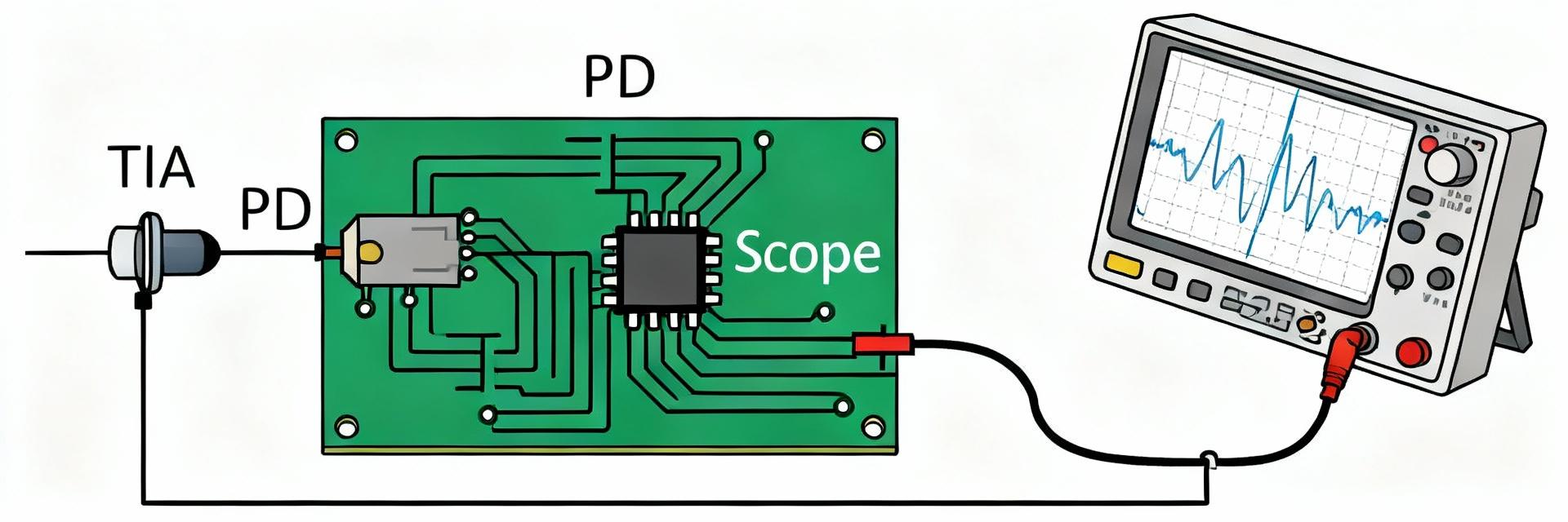
Test Setup & Measurement Methodology
Recommended testbench and instruments
Point: A low-noise testbench is required to reveal true device limits. Evidence: Use a calibrated low-current source or optical calibrated source for photodiodes, precision feedback resistors, low-noise supplies, high-resolution scope/digitizer, spectrum analyzer for noise density, and picoammeter for DC checks. Explanation: Proper shielding, star grounding, and a PCB fixture with short traces and local decoupling minimize parasitics that would otherwise mask intrinsic noise and stability behavior.
Step-by-step measurement procedures and pass/fail criteria
Point: Define repeatable procedures and clear acceptance criteria. Evidence: Measure transimpedance by injecting known current and recording Vout (TIA gain = Vout/Iin); assess input-referred noise as noise density (fA/√Hz) integrated to RMS over bandwidth; find -3 dB point on gain vs frequency; evaluate linearity by stepped input and report THD or deviation percentage. Explanation: Use averaging, multiple samples, and calibrated references; declare typical vs guaranteed margins and list pass/fail thresholds tied to system-level error budgets.
TPA8801B-TR — Measured Performance, Specs & Limits
Transimpedance gain, stability, and typical vs. limit values
Point: Present transimpedance as population statistics and conditions. Evidence: Report typical, min/max and spread across units, and show gain vs frequency and gain vs feedback resistor plots; include gain drift with temperature. Explanation: Comparing measured DC gain to datasheet claims requires documenting supply rails, resistor tolerance, and test load; stability assessment uses phase margin and observation of oscillation under worst-case parasitic capacitance.
Noise, bandwidth, linearity and output drive limits
Point: Quantify noise performance and dynamic limits for system integration. Evidence: Provide input-referred noise density plots (fA/√Hz), integrated noise (pA RMS) over specified bandwidth, measured -3 dB bandwidth, linearity deviation vs input, and output swing under load. Explanation: These results identify practical limits (saturation and output clamp regions) and show how feedback resistor selection affects noise vs bandwidth trade-offs; a measured-vs-datasheet table clarifies margin under stated conditions.
Edge Cases, Thermal Behavior & Failure Modes
Stress tests, thermal derating and reliability indicators
Point: Thermal and stress tests reveal long-term and corner behavior. Evidence: Elevated-temperature cycling, sustained input overdrive, and power-cycling expose gain shifts, increased noise, or offset drift; thermal imaging highlights hot spots on the package and PCB. Explanation: Plotting metric change vs temperature/time quantifies derating curves and sets operational limits; specify when to derate feedback resistor or reduce supply headroom to maintain specs.
Protection, overload behavior and recovery
Point: Characterize overload response and recovery to define safe operating area. Evidence: When inputs exceed recommended ranges some devices exhibit input clamp action, output limiting, or slow recovery; document clamp thresholds and recovery time under incremental overstress. Explanation: Define test sequences to map safe zones and recommend PCB-level protections (series resistor, input filtering, clamp patterns) to avoid performance degradation without naming specific external parts.
Application Guidance & Integration Checklist
Board-level integration checklist and recommended configurations
Point: Provide a concise checklist for reliable integration. Evidence: Key items include feedback resistor trade-offs (gain vs bandwidth vs noise), short input traces, continuous ground planes, local decoupling next to supply pins, and input ESD/filter patterns. Explanation: Two example briefs—high-sensitivity mode (large Rf, tight shielding, narrow bandwidth) and wide-band mode (smaller Rf, controlled decoupling, attention to phase margin)—help engineers pick resistor and decoupling approaches without specific component references.
When to use this device and alternatives to evaluate
Point: Summarize ideal use cases and trade-offs. Evidence: The device is well-suited for low-current photodiode readout where noise performance outweighs bandwidth; conversely, very wide-band applications may favor lower-gain front ends. Explanation: Evaluate alternatives by comparing sensitivity, noise floor, bandwidth, package, and thermal constraints; add evaluation checklist items for prototype comparisons and cost/complexity trade-offs.
Summary
- Measured transimpedance and stability present consistent typical gains across samples; design must trade feedback resistor for bandwidth and noise to meet system specs.
- Noise performance and -3 dB bandwidth define realistic detection limits; thermal tests show measurable drift that requires derating for elevated ambient conditions.
- Board layout and input protection patterns materially affect achievable specs; follow the checklist to avoid parasitic-induced instability and output saturation.
FAQ: TPA8801B-TR measured specs — How reproducible are the main results?
Point: Reproducibility depends on test discipline. Evidence: With calibrated sources, shielding, and multiple samples, typical transimpedance and noise figures repeat within published spreads. Explanation: To achieve similar reproducibility, use the same resistor tolerances, document supply rails, and report bandwidths and averaging used in the measurement; share raw CSV and plots for verification.
FAQ: What is the TPA8801B-TR noise performance in system terms?
Point: Convert device noise into system-limited detection. Evidence: Input-referred noise density integrated over the detector bandwidth yields RMS current noise (pA RMS), which combines with sensor shot noise to set minimal detectable signal. Explanation: Use the provided noise density plots and integrate to the application bandwidth to confirm whether the front end or the sensor dominates the noise budget.
FAQ: How should I test TPA8801B-TR bandwidth limit for my application?
Point: Bandwidth testing must match real-world loading. Evidence: Measure gain vs frequency with the chosen feedback resistor and expected input capacitance, then determine the -3 dB point and phase margin. Explanation: If the measured -3 dB point is below system needs, reduce feedback resistance or minimize input capacitance, and re-evaluate stability with the actual PCB layout and source impedance.


