
The following is a focused, data-first digest intended to let engineers judge fit in minutes. Quick snapshot: this device is a compact high-side current-sense amplifier with voltage output, integrated comparator and internal reference — reported supply range is ~1.3–5.5 V and it is available in an 8-pin small-outline package. This brief pulls the datasheet’s critical numbers and gives actionable integration tips and a short design checklist for fast evaluation.
1 — Device background: what it is and where it fits (background introduction)
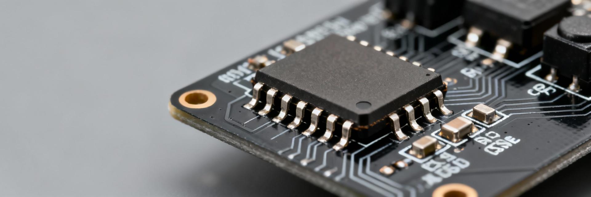
Core function & internal blocks
At core, the part implements a high-side current-sense amplifier path (sense input → precision amplifier → voltage output), an on-chip comparator path that references the internal voltage reference, and supporting biasing. The amplifier converts small differential sense voltages across a sense resistor into a single-ended voltage suitable for ADCs or logic-level comparators; the internal comparator can produce a threshold-based digital flag. Package style is an 8-pin MSOP/TSSOP form-factor and the typical operating supply range supports low-voltage battery systems. See the Electrical Characteristics table in the datasheet for exact performance tables.
Target applications and system-level role
Typical applications include battery and charger monitoring, buck-converter current telemetry, overcurrent detection and general power-management sensing. Engineers choose this class of device for high-side sensing where placing the sense resistor at the supply rail simplifies system topology; the integrated comparator and reference reduce external component count and software polling. Limitations to call out: insertion loss across Rsense, comparator input range vs. common-mode, and thermal derating at higher currents.
2 — Quick specs snapshot (data analysis)
Critical electrical specifications to list
Key specs to extract for quick go/no-go: supply voltage range, input common-mode range, amplifier gain/sensitivity, comparator thresholds and hysteresis behavior, quiescent current, input offset/accuracy, bandwidth, output swing versus supply, absolute maximums and operating temperature range. Presenting these as a compact reference makes initial decisions fast.
| Parameter | Typical/Example |
|---|---|
| Supply voltage | ~1.3–5.5 V (check Electrical Characteristics) |
| Input common-mode | High-side up to VCC (see datasheet) |
| Gain / sensitivity | Device-defined; use datasheet gain or sensitivity figure |
| Comparator thresholds | Internal reference-based; programmable via resistor divider |
| Quiescent current | Low-µA range (see datasheet table) |
| Offset / accuracy | Spec’d in Electrical Characteristics |
| Bandwidth / response | Limited to audio/low-MHz range depending on gain |
| Output swing | Near-ground to (VCC – headroom) |
| Package / thermal | 8-pin MSOP/TSSOP; check θJA for thermal limits |
| Temperature range | Industrial or commercial per datasheet |
Package, pinout & thermal limits
Include a concise pin-function table (VCC, GND, IN+, IN–/sense, OUT, COMP, REF adjust, NC/pin). Recommended notes: follow the vendor land-pattern, place VCC bypass caps within 1–2 mm of VCC pin, and consult the thermal resistance (θJA) entry to calculate allowed power dissipation. For mechanical layout use the datasheet footprint and recommended solder-mask openings; avoid assuming thermal relief without checking θJA for your board copper.
3 — Design & integration guide (method/how-to)
Circuit-level design tips
Sense resistor selection template: Rsense = Vsense_max / Imax where Vsense_max respects amplifier input range and power loss budget. Example trade-off: reducing Rsense improves efficiency but lowers measurable V, requiring higher gain and potentially higher offset error. Use the comparator with a resistor-divider to set trip thresholds referenced to the internal reference; add hysteresis either via a small positive feedback resistor or external RC to prevent chatter. Recommended decoupling is 0.1 µF + 1 µF at VCC; add series input filtering (RC) to suppress current-sensing spikes but ensure bandwidth remains sufficient for detection.
PCB layout and thermal/ESD considerations
Keep sense traces short and wide; if possible use Kelvin-sense traces to separate sense-node measurement from current-carrying copper. Place bypass capacitors adjacent to VCC pin. Use copper pours to aid thermal dissipation and avoid routing high-current paths under sensitive analog traces. Add an input TVS or series resistor for ESD protection if the environment is harsh. Recommended bench test points: sense resistor voltage, amplifier output, comparator output and VREF node.
4 — Example use cases & quick circuits (case display)
Example: battery-powered current monitoring
Worked example (numeric): target measurable range 0–5 A, assume allowable Vsense_max = 250 mV to limit power loss. Choose Rsense = 250 mV / 5 A = 0.05 Ω (50 mΩ). If the amplifier effective gain is 20, Vout_max ≈ 20 × 0.25 V = 5.0 V — ensure Vout_max does not exceed ADC input or device output swing at your VCC. Comparator trip: to detect 3 A trip, set comparator threshold to Vsense_trip = 3 A × 0.05 Ω = 0.15 V; adjust resistor divider to generate that threshold relative to internal reference. Validate with a ramp test and oscilloscope to confirm expected waveforms and comparator hysteresis behavior.
Example: power-management trip/protection application
Block-level: sense → amplifier → comparator → MCU interrupt or MOSFET gate driver. The comparator latency is usually microseconds; account for any propagation delay and filtering when specifying trip response. Typical failure modes: transient spikes causing false trips, thermal drift shifting offset, and comparator output not compatible with downstream logic levels — confirm output type and pull-up requirements in the datasheet.
5 — Quick checklist & troubleshooting (action advice)
Datasheet checklist for quick validation
Design-review checklist: verify supply range and quiescent current in Electrical Characteristics; confirm input common-mode and offset specs; check comparator thresholds and output type; confirm package pinout and footprint; validate absolute maximums and thermal derating via Absolute Maximum Ratings and θJA entries; and confirm that chosen Rsense produces acceptable power loss. Use the key specs table above as the fast reference during procurement and design review.
Bench troubleshooting & test procedures
Lab tests: measure quiescent current at nominal VCC (compare to datasheet), inject a known current through Rsense and verify amplifier Vout vs. expected value (allowing for offset), perform a comparator ramp test to find trip threshold and hysteresis, and if possible run temperature sweep to check drift. Tolerances: expect output within datasheet offset ± specified error; large deviations indicate layout, grounding, or damaged device.
Summary
TPA2295CT-VS1R-S is a compact high-side current-sense amplifier with integrated comparator and reference; its suitability depends on supply range, amplifier accuracy and comparator behavior relative to the target battery or power-management system. Use the quick specs table and design checklist above to rapidly validate the part against system constraints, and apply the worked example to size Rsense and comparator thresholds. For final integration, download the official product datasheet from the product page and cross-check the values used in your design.


