
Measured input-referred noise, typical common‑mode rejection ratios spanning tens of dB, and gain accuracy figures from multiple datasheet tables explain why the TPA9361-SO1R is chosen for precision signal conditioning. This deep dive quantifies the device’s performance envelope and sets up repeatable bench tests designers can use to validate claimed behavior in real designs.
This article is written for design and test engineers who must translate datasheet numbers into system error budgets and repeatable validation steps. Readers will get a prioritized spec checklist, worked calculations for power and offset impact, and step‑by‑step methods to reproduce noise, CMRR and PSRR results on the bench.
1 — Device overview & typical applications (background)
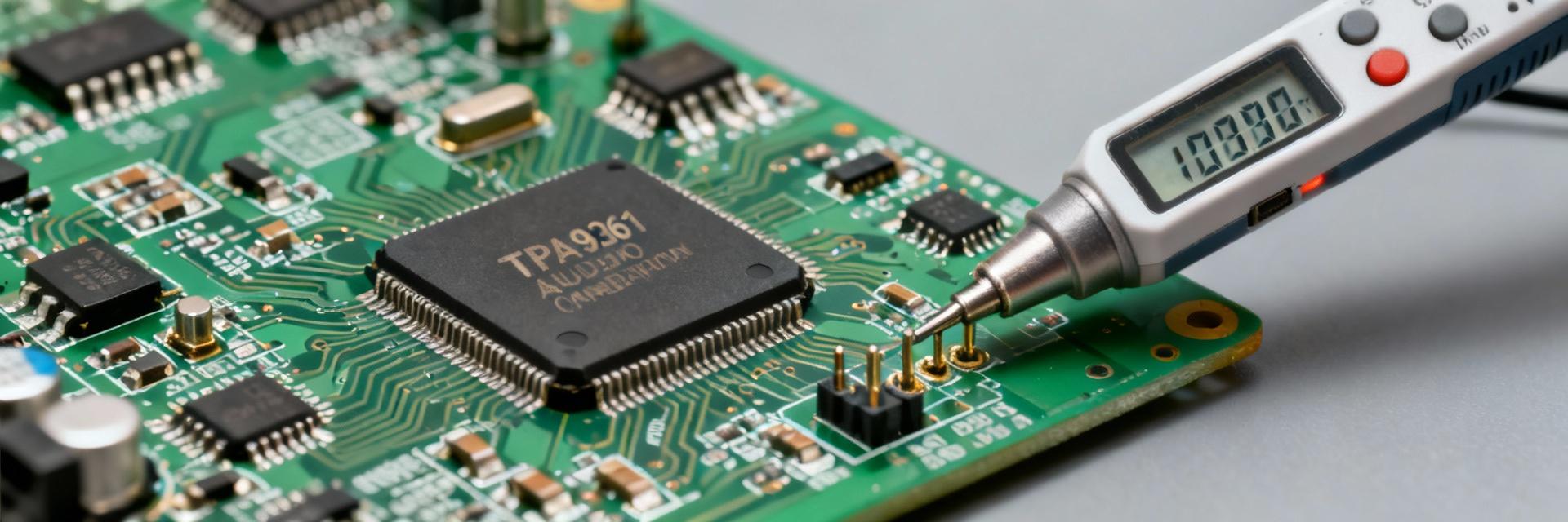
What the TPA9361-SO1R is and why it matters
The TPA9361-SO1R is a fixed‑gain difference amplifier / precision signal conditioner intended as an ADC front end and sensor interface. The datasheet lists typical gains, input and common‑mode ranges, and package thermal notes that influence footprint and PCB thermal relief. Designers should extract package pin‑count and maximum junction-to-ambient derating from the device documentation before layout.
Key block-level features to extract from the datasheet
Capture: nominal gain, gain tolerance, input common‑mode range, supply range, input offset and drift, input‑referred noise density, bandwidth, CMRR vs frequency, PSRR, supply currents, and absolute vs recommended ratings. Produce a short checklist or table showing typical vs maximum values and conditions (temp, supply) so reviewers can quickly compare candidates.
2 — Electrical specs deep-dive: accuracy & signal integrity (data analysis)
Gain accuracy, offset, drift — what they mean in practice
Gain tolerance and offset error define the static portion of the system error budget. Use datasheet typical and max columns to compute worst‑case error at the ADC input: worst‑case offset plus gain error scaled by full‑scale input produces LSB loss. Include temp coefficient (offset drift) to project error over required operating temperatures for a complete accuracy budget.
Noise, bandwidth, CMRR, and PSRR implications
Read noise density and integrated noise over your ADC bandwidth to predict RMS error. Convert noise density (nV/√Hz) to RMS by integrating over the effective bandwidth. Reproduce CMRR and PSRR tables as plots to see frequency dependence; low‑frequency PSRR and midband CMRR are often the limiting factors for precision sensor interfaces.
3 — Power, thermal, and reliability constraints (data analysis / methods)
Supply currents, power dissipation, and thermal derating
Pull typical and max supply currents and operating voltages from the datasheet and compute dissipation: P = VCC × ICC (plus any other rails). Compare that to package thermal resistance and ambient conditions to calculate junction temperature and allowable derating. Use a worked example for your supply to verify the SO1R package stays below safe junction limits under worst‑case loading.
Absolute maximums, ESD ratings, and recommended operating conditions
Differentiate absolute maximum ratings from recommended operating conditions to define safe margins. Apply conservative derating (10–20%) on voltages and junction temps for reliability and consider ESD handling and input protection needs during test and production. Document margin strategies in the design review checklist.
4 — Bench test procedures to validate key specs (methods / tests)
Repeatable tests for gain, offset, and drift
Use a low‑noise precision source, buffered single‑ended and differential input fixtures, and a high‑resolution ADC or DMM. Define test points: DC offset at multiple supplies, gain with known differential voltages, and temperature points for drift. Capture averages and standard deviations, and include instrument uncertainties into the final error budget.
Measuring noise, CMRR, bandwidth, and PSRR
For noise, use FFT averaging with a spectrum analyzer or digitizer and integrate the noise density across the ADC bandwidth. For CMRR perform differential injection with a common‑mode source and measure rejection vs frequency. For PSRR inject a modulated supply tone and measure output modulation. Watch for ground loops and probe loading; use proper termination and shielding.
5 — Application examples & design trade-offs (case / comparison)
Typical front-end configurations and layout considerations
Two concise examples: a differential sensor interface with series input resistors and anti‑aliasing RC, and an ADC driver with matched input network and low‑ESR bypass caps. Emphasize short feedback paths, local power decoupling, and guard routing for high‑impedance nodes. Early PCB prototypes should validate leakage and common‑mode behavior on the actual board.
Trade-offs: accuracy vs. bandwidth vs. power
Increasing bandwidth typically raises integrated noise and may require higher power; adding filtering reduces bandwidth but improves noise. Lowering supply or bias currents reduces power but can degrade linearity and offset. Choose configuration based on the application’s dominant constraint—noise floor, update rate, or energy budget—and validate with the prescribed bench tests.
6 — Practical checklist & recommended tests for qualification (action)
Quick pre-silicon / pre-layout spec checklist
Verify supply range, input/common‑mode limits, required headroom for the signal, offset and noise budget, thermal dissipation for the chosen package, and required margins against absolute maximums. Reference the device identification and the official datasheet entries when logging checklist results so reviewers can trace each spec back to its source in documentation.
Post-layout and production test recommendations
For prototype sign‑off run DC offset, gain, basic noise spot checks, and a thermal soak with logged junction temps. For a minimal production test suite include automated DC checks, a short FFT noise check, and a PSRR spot test. Log lot/date, assembly ID, and key measured metrics for traceability and regression analysis.
Summary
Key datasheet elements that govern real‑world performance are gain accuracy, input‑referred noise, CMRR/PSRR vs frequency, and thermal limits; extracting these numbers and folding them into system error budgets is essential. Use the outlined bench procedures to validate claimed specs, prioritize offset and noise tests for precision front ends, and confirm thermal margins on the target board for safe operation of TPA9361-SO1R.
FAQ
What basic equipment is needed to measure offset and gain?
A low‑noise precision source, a stable reference ADC or calibrated DMM, proper input buffering for single‑ended and differential modes, and controlled temperature conditions are required. Use averaging and uncertainty budgeting to separate instrument error from the device under test and document settings for repeatability.
How should I approach measuring input-referred noise?
Capture a noise spectrum with a digitizer or spectrum analyzer, apply windowing and averaging to reduce variance, and integrate the noise density across the effective bandwidth of your ADC. Ensure source and termination noise are below the device under test and account for instrument noise in the final result.
What are common pitfalls when measuring CMRR and PSRR?
Pitfalls include improper common‑mode injection, ground loops, probe loading, and insufficient supply decoupling. Use a dedicated common‑mode source for CMRR, inject a small modulated tone for PSRR, and isolate grounds. Repeat measurements at multiple frequencies to reveal frequency‑dependent behavior that can affect system performance.


