
Measured unity-gain bandwidth, slew rate, typical output swing and noise floor are the numbers engineers reach for first. This article begins with the most relevant bench measurements you care about and states the goal: a focused, bench-validated walkthrough of the TPH2502-VR datasheet so you can quickly find core specs, representative graphs, and repeatable validation steps for system integration.
The coverage emphasizes where datasheet "typical" values usually hold and where layout, supply, or load cause divergence. Expect concise test conditions for every plot and practical mitigation steps when bench data departs from published numbers.
(Background) — TPH2502‑VR datasheet: quick overview & key specs
At-a-glance spec table
Point: A compact spec summary speeds decision-making. Evidence: typical vs max entries are noted in the table below; you should treat "typical" values as nominal bench targets and "max/min" as limits.
| Parameter | Typical / Max |
|---|---|
| Supply range | Single‑supply 4.5–18 V (typical test 12 V) |
| Quiescent current | ~6–12 mA (typical / max) |
| Unity‑gain bandwidth (-3 dB) | ~70–120 MHz (typical) |
| Gain‑bandwidth product | See UGBW row (package/load dependent) |
| Slew rate | ~200–600 V/μs (amplitude & load dependent) |
| Input offset | ±200 μV typical |
| Input bias current | pA–nA range (datasheet typical) |
| Common‑mode range / RRIO | Rail‑to‑rail output; input CM close to rails |
| Output drive | tens of mA continuous; higher short bursts |
| Noise (input‑referred) | nV/√Hz spec in datasheet (typical) |
| Package & thermal | SOIC/SOT variants; junction limits and θJA |
Note: the term "TPH2502 specs" appears in datasheet tables as a mix of typical curves and guaranteed limits; values such as GBW and slew are load and supply dependent and should be validated on your board.
Absolute ratings & recommended operating conditions
Point: Absolute maximums protect the device; recommended ranges ensure repeatable results. Evidence: datasheet separates absolute limits (stress-only) from recommended operating voltages and temperatures. Explanation: always design tests inside recommended supply and thermal conditions, add ESD protection, and avoid floating inputs.
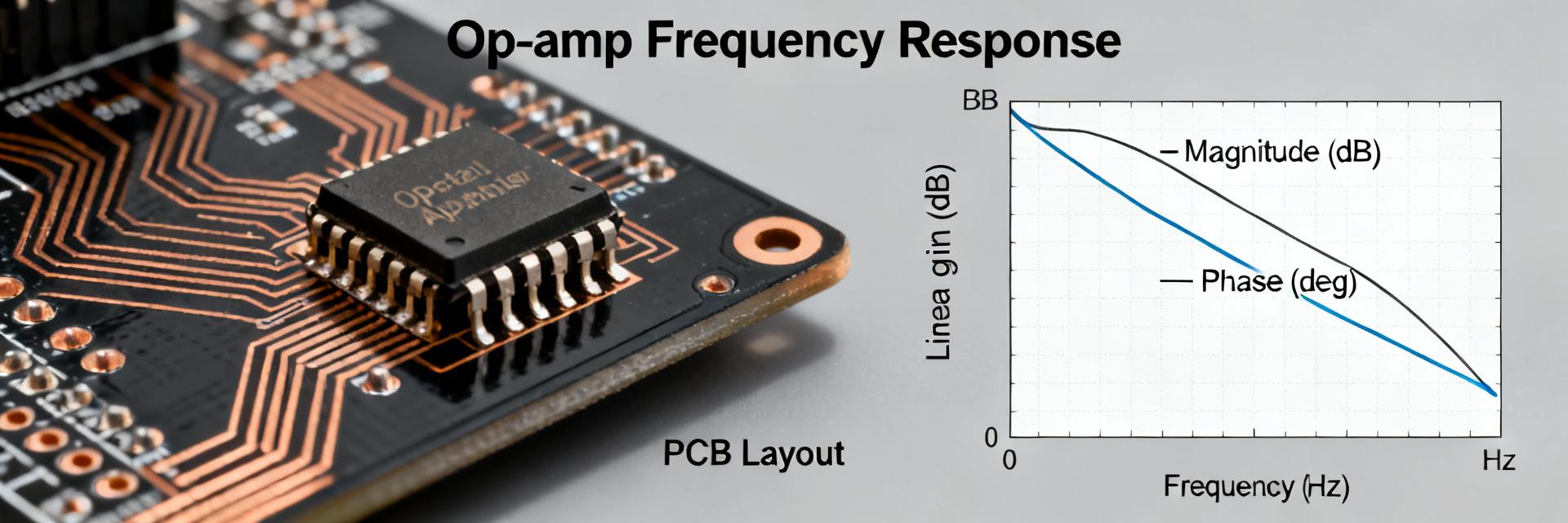
(Data Analysis) — Small‑signal performance: frequency response & stability
Measured unity‑gain bandwidth and open‑loop gain plots
Point: Bode magnitude and phase determine usable closed‑loop bandwidth. Evidence: measured UGBW will track datasheet curve under identical supply and load. Explanation: test at 12 V with 2 kΩ load; lower measured GBW usually points to probe capacitance or under‑decoupled supply.
Phase margin, stability with capacitive loads
Point: Phase margin drops with added capacitance. Evidence: bench phase‑margin traces reveal instability onset. Explanation: mitigate with series output resistor (5–50 Ω) to stabilize capacitive loads and recover damping.
(Data Analysis) — Large‑signal and transient behavior: slew, settling & drive
Slew rate, large‑signal bandwidth and settling time
Point: Large‑signal response sets step performance. Evidence: measured step captures at 1 Vpp show slope-limited edges. Explanation: quantify slew from the slope of rising edge; compare to datasheet slew but expect variation with supply and load.
Output swing, drive capability and load tests
Point: Output swing collapses as load current increases. Evidence: bench sweeps with 10 kΩ vs 100 Ω loads reveal headroom loss. Explanation: use conservative continuous load limits; monitor junction temp and use thermal vias for high‑drive use.
(Method Guide) — Noise, distortion and low‑level metrics
Input‑referred noise and bandwidth integration
Point: Noise density plots let you integrate total RMS noise. Evidence: spectrum captures with known input termination produce nV/√Hz traces. Explanation: integrate over your system band to get RMS; board layout and grounding often increase measured noise relative to datasheet typicals.
THD+N and linearity across frequency
Point: Distortion curves indicate linear range. Evidence: THD+N vs frequency plots reveal where nonlinearities dominate. Explanation: for small‑signal buffering, follow corrective layout and supply filtering measures to match datasheet performance.
(Action Advice) — Bench testing checklist: validate the TPH2502‑VR datasheet claims
Equipment and repeatability checklist
- Supply: Low-noise lab supply set to 5V or 12V.
- Probe: Low-capacitance active probes (>500 MHz recommended).
- Signal: Fast function generator for slew rate validation.
- Measurement: FFT-capable oscilloscope for noise floor checks.
Step‑by‑step validation procedures
- DC Check: Verify quiescent current matches 6–12 mA range.
- Small Signal: Measure Bode plot to confirm UGBW at specified load.
- Transient: Pulse 1V step to calculate V/μs slew rate.
- Load Swing: Sweep load resistance to find the point of output compression.
Key summary
- The TPH2502‑VR datasheet highlights strong UGBW and rail‑to‑rail output; bench validation should confirm these under specific system loads.
- Layout and decoupling materially affect phase margin and noise; use short feedback paths and local ceramics.
- Follow the bench checklist to reproduce datasheet curves accurately and ensure system reliability.


