The TPA6551N-S6TR is a compact, single-supply buffer/amplifier optimized for portable audio and precision instrumentation. Its SOT-23-6 package facilitates rapid PCB integration and short revision cycles. This guide distills essential datasheet parameters into a practical one-page reference for hardware engineers.
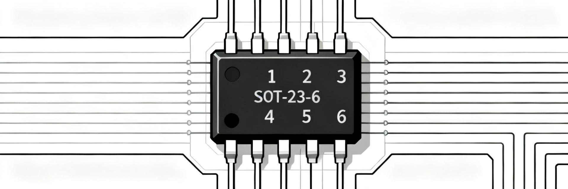
Background & Key Features
Targeted at low-voltage environments, the TPA6551N-S6TR manages signal conditioning in battery-powered devices. It features an internal structure optimized for high input impedance and stable output driving capabilities.
| Parameter | Specification / Design Notes |
|---|---|
| Supply Voltage Range | 2.7V – 5.5V (Single Supply) |
| Max Output Drive | Check guaranteed limits for short-circuit protection |
| Common-Mode Range | Rail-to-Rail dependent; verify input biasing |
| Quiescent Current | Low-power active and standby modes |
| Package Type | SOT-23-6 (Small Outline Transistor) |
| Operating Temp | Industrial Grade (-40°C to +85°C/125°C) |
Detailed Pinout & Functions
| Pin # | Name | Type | Function & Wiring Notes |
|---|---|---|---|
| 1 | IN+ | Input | Non-inverting input; maintain high impedance |
| 2 | IN− | Input | Inverting input for feedback loops |
| 3 | OUT | Output | Low-impedance driver; keep traces short |
| 4 | VCC | Power | Decouple with 0.1µF close to pin |
| 5 | GND | Ground | Solid ground plane connection |
| 6 | BYPS/COMP | Ref | Bypass or compensation; follow datasheet cap values |
Thermal & Layout Best Practices
Efficient thermal management is critical for the SOT-23-6 package. Use the formula Pmax ≈ (Tj_max − Ta)/θJA to verify safety margins. Place decoupling capacitors within 2mm of the VCC pin and utilize a ground pour to minimize EMI and parasitic oscillation.
Quick Troubleshooting
What are common pinout mistakes when using the TPA6551N-S6TR?
Which datasheet values should be used for worst-case design?
How should I verify performance on the first prototype?
What is the recommended decoupling for the VCC pin?
Summary Checklist
- Power: Verify 2.7–5.5V range and local decoupling.
- Signal: Ensure input bias is within common-mode limits.
- Thermal: Calculate θJA vs. expected load current.
- Layout: Confirm Pin 1 orientation on PCB footprint matches datasheet.