
Ultra-low offset and pA-range input bias currents for precision front-ends and low-noise buffers.
The device delivers ultra-low offset (tens of microvolts in typical conditions) and pA‑range input bias currents, metrics that matter when designing precision front-ends and low‑noise buffers. Those orders of magnitude reduce calibration needs and preserve sensor dynamic range in high‑gain chains, so engineers choose the part where drift and leakage dominate error budgets.
This article unpacks the electrical specs, package and pinout, integration tips and bench test checks so teams can evaluate and implement the device quickly. It highlights where to verify datasheet numbers, how to format a spec table for review, and what PCB and test practices confirm the published specs and recommended pinout.
(1) Background & Key Use Cases (Background introduction type)
What the part is and where it fits
The component is a zero‑drift, low‑offset amplifier/buffer optimized as a low‑offset buffer for sensor front‑end designs and precision I/O. Its class‑level behaviors—near‑zero offset, low offset drift, and very low input bias—make it a fit for instrumentation, precision ADC drivers and low‑leakage I/O where the published specs determine usable resolution and required calibration frequency.
Typical application scenarios and selection criteria
- •Precision sensor front‑ends: choose when Vos, Vos drift and input bias current dominate error; evaluate offset and drift specs against system resolution and calibration cadence.
- •Low‑noise buffer/amplifier: select when noise density, slew rate and GBW must support the sensor bandwidth without adding instability.
- •Leakage‑sensitive I/O and instrumentation: prioritize low input bias current, wide common‑mode range and single‑supply operation for simplified power rails and reduced board complexity.
(2) TPA5521-DFPR — Electrical Specifications (Data analysis type)
DC electrical data (what to tabulate)
| Parameter | Typical | Maximum / Notes |
|---|---|---|
| Input offset voltage (Vos) | datasheet value (TA, VCC) | datasheet value (test conditions) |
| Input bias current | datasheet value (TA, VCC) | datasheet value |
| Offset drift (dVos/dT) | datasheet value | datasheet value |
| Input / output voltage range | datasheet value | with RL and VCC |
| Supply voltage range | datasheet value | min–max |
| Quiescent current | datasheet value | per channel |
| Common‑mode range | datasheet value | note test circuit |
Use the table to copy exact datasheet numbers and annotate TA, VCC, RL and test configuration. For design reviews, include measurement tolerances and the test fixture used to report each DC spec so comparisons are apples‑to‑apples.
AC and dynamic characteristics
Tabulate GBW, slew rate, phase margin (with typical feedback networks), and noise density. Provide a compact comparison of typical versus maximum values to reveal headroom for closed‑loop gains; note the test amplifier configuration (unity buffer, gain of 10, RL value) used to define each AC spec and any compensation or output series resistance required for stability.
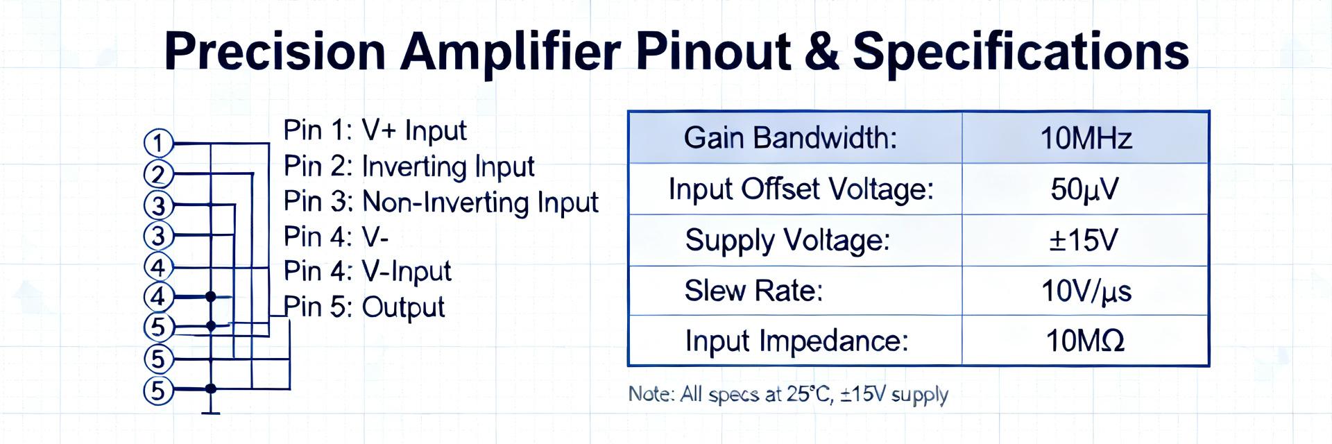
(3) TPA5521-DFPR — Package, Pinout & Thermal (Data/case type)
Package mechanical details and footprint guidance
The part is supplied in a 4‑XFDFN style package with an exposed thermal pad. For PCB footprint guidance use the mechanical drawing from the official package data and follow recommended land pattern and solder mask openings. Include an SVG or high‑resolution outline for layout review and verify courtyard, solder fillet and stencil aperture sizes against the mechanical tolerances in the datasheet.
Pinout table and pad functions + thermal considerations
| Pad | Name | Dir | Function / Notes |
|---|---|---|---|
| 1 | IN+ | IN | Non‑inverting input — route short, protect from leakage and contamination |
| 2 | IN− | IN | Inverting input — match impedance and keep feedback return short |
| 3 | OUT | OUT | Output — consider series R for stability into capacitive loads |
| 4 | VCC | POWER | Supply — decouple close to pad |
| EP | Exposed Pad | GND/Thermal | Ground/thermal; follow soldering notes and thermal via pattern |
Populate exact pin numbers and names from the datasheet for final documentation. For thermal performance, follow recommended exposed pad soldering, add thermal vias to a ground plane and compute θJA per mounting style to ensure derating targets are met.
(4) Design Integration & Typical Application Circuits (Method guide type)
Reference circuits and BOM highlights
Provide three reference circuits: unity‑gain buffer for ADC drive, low‑noise amplifier for sensor with low‑value feedback resistor and single‑supply instrumentation front‑end with level shifting. For each, call out critical passives (input protection diodes or series resistors, feedback resistor values, Ccomp for stability) and a minimal BOM emphasizing precision resistor tolerances, low‑ESR decoupling and COG/NPO capacitors where required.
Layout, decoupling and stability tips
- Place decoupling caps within 1–2 mm of VCC pin.
- Route inputs as short guarded traces.
- Keep feedback loop area minimal.
- Use a single ground plane with a solid return under the package.
- Add a small output series resistor (10–100 Ω) when driving capacitive loads.
- Use local 0.1 µF and 1 µF decoupling to suppress supply impedance peaks.
(5) Testing, Troubleshooting & Best Practices (Action advice type)
Bench test procedures to validate specs
Suggested test flow: 1) verify quiescent current and supply range with a precision DMM and regulated source; 2) measure Vos using a chopper‑stable null setup and a μV‑capable DMM; 3) measure input bias with picoammeter and guarded fixtures; 4) sweep frequency for GBW and measure noise density with a low‑noise spectrum analyzer. Note probe loading and fixture leakage can dominate low‑bias measurements.
Common failure modes and fixes
Symptoms and fixes: oscillation often traces to long feedback traces or missing output series resistor—add Rseries or tighten layout; excess offset drift can indicate thermal gradients or contaminated inputs—add shielding and cleaning; elevated supply current suggests ESD damage or solder bridging—inspect board and replace parts. Follow ESD handling procedures for exposed‑pad packages.
SEO Notes: Target long‑tails such as "TPA5521-DFPR electrical specs table" and "TPA5521-DFPR pinout diagram 4-XFDFN" in metadata.
Suggested Meta Description: "Complete TPA5521-DFPR guide: key electrical specs, package & pinout, integration tips and test procedures for precision amplifier designs." Ensure datasheet and mechanical files are linked from the live article for download and reference in the prototype phase.


