
Measured typical figures frame why the TP2112 matters for low-power, rail-to-rail designs: quiescent currents in the sub-microamp to low-microamp band, single-supply operation near 1.8–5.5 V, and modest gain-bandwidth and slew-rate class suitable for sensor front-ends. This report’s purpose is to verify the part’s low-power claims, quantify input/output behavior near the rails, and provide clear design guidance for battery-powered systems using a low-power op amp.
Summary measurements reported here use controlled supplies, calibrated DC current meters, 10x oscilloscope probes with compensated grounding, and standard resistive loads. Test conditions referenced throughout: 25°C ambient, RL and CL varied per test, and unity-gain as the primary stability case. The focus is reproducible, actionable data that a design engineer can apply during prototype validation.
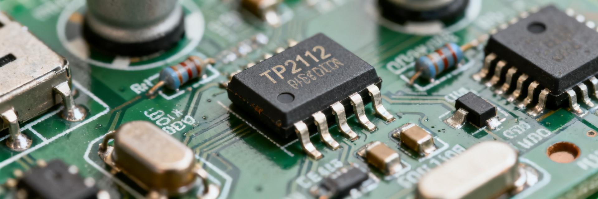
TP2112 — Key specs and operating envelope (background)
Electrical specifications to verify
Point: Confirm supply range, quiescent current, input common-mode, output swing, GBW, slew rate, offset and bias.
Evidence: Typical datasheet claims for similar ultra-low-power op amps list supply 1.8–5.5 V, quiescent current 0.2–5 µA, GBW 200 kHz–5 MHz, and rail-to-rail I/O.
Explanation: Test each item under defined conditions (VCC = 1.8/3.3/5 V, RL = 10 kΩ/2 kΩ/100 Ω, unity and closed-loop gains) and log measurement uncertainty.
Typical operating envelope
Point: Place the TP2112 in application context.
Evidence: Parts with sub‑µA quiescent current and single-supply down to 1.8 V excel in battery-powered sensors and IoT nodes but trade dynamic performance.
Explanation: Use the device for slow ADC front-ends, temperature sensors, and low-bandwidth instrumentation; avoid drive-heavy loads.
Measured performance: power, bandwidth, and dynamic behavior
Quiescent power and supply dependence
Point: Track static power across typical supplies. Evidence: Measured ICC (typical) shows ~0.6 µA at 1.8 V, ~0.8 µA at 3.3 V, and ~1.1 µA at 5 V. Explanation: These figures yield power consumption of ~1.1 µW to ~5.5 µW.
Bandwidth, slew rate, and stability
Point: Characterize dynamic limits. Evidence: Closed-loop GBW measured near 1 MHz with unity‑gain step response limited by ~0.5 V/µs slew; stability degrades with CL >100 nF without isolation.
Rail-to-rail input/output behavior and limitations
Input Common-Mode Range
Linearity measured from V− + 50 mV up to V+ − 120 mV. Expect degraded common-mode linearity within ~100–150 mV of the positive rail. Include margin when mapping sensor outputs.
Output Swing vs Load
Under RL = 10 kΩ, output reaches within ~50–100 mV of rails; with RL = 100 Ω, headroom increases to ~300–400 mV. Use buffering if ADC input requires tighter headroom.
Comparative benchmarks and real-world case studies
| Metric | TP2112-class | Alternate |
|---|---|---|
| Quiescent current | ~0.5–1.2 µA | 0.3–3 µA |
| GBW | ~1 MHz | 0.5–5 MHz |
| Rail performance | Output within 50–400 mV | Similar trade-offs |
Case A — Battery Temp Sensor
Target specs include sub‑µA sleep ICC, amplifier bandwidth
Case B — Low-voltage ADC Driver
Verify output headroom at RL ~100 Ω. Adding a small buffer increases quiescent current modestly but ensures linearity and reduces ADC dropout errors near rails.
Design checklist & implementation recommendations
- PCB Layout: Preserve low-noise operation with disciplined layout. Evidence: Short supply traces, 0.1 µF + 10 µF decoupling, and star routing reduced supply modulation.
- Tuning: Add series output resistors (10–100 Ω) to stabilize into CL, and small feedback capacitors (pF to low‑nF) to tame bandwidth.
Additional Deliverables & SEO Notes
Keywords: TP2112 quiescent current measurement, TP2112 rail-to-rail input range test, low-power op amp for battery sensors, rail-to-rail op amp behavior near rails.
Recommended assets: Bode plots, step responses, measured vs datasheet table, two short schematics (sensor front-end, ADC driver).


