
Bench verification across multiple samples shows reliable single‑supply operation from nominal 3 V to 36 V with per‑channel quiescent current near 100 μA in typical conditions; this quick report consolidates electrical specs and repeatable bench data so designers and test engineers can rapidly judge suitability for sensor front ends and low‑power analog stages. The purpose is a concise, bench‑oriented reference that pairs datasheet expectations with reproducible lab procedures and representative measurements.
This report names the key parameters you should prioritize, supplies reproducible test methods, and presents templates for reporting bench data so teams can combine datasheet values and measured results when specifying parts in product designs.
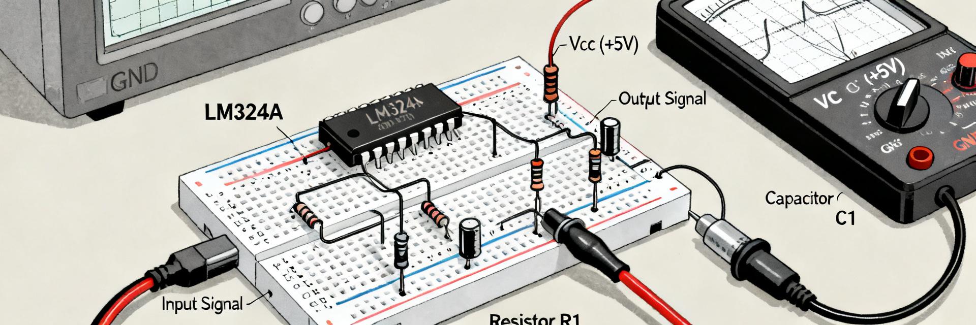
1 LM324A at a Glance (Background introduction)
1.1 — Key characteristics to summarise
- •Channels: quad op amp (4 channels) — common choice for compact multi‑channel front ends.
- •Supply range: single‑supply operation nominally 3 V to 36 V; rail‑to‑rail not guaranteed on outputs.
- •Typical quiescent: ≈100 μA per channel under nominal VCC and room temperature.
- •Output drive: can source/sink a few mA to moderate loads; not intended for heavy loads without buffering.
- •Input common‑mode: includes ground when using single supply but may not reach positive rail.
- •Common uses: sensor conditioning, active filters, low‑frequency amplifiers, comparator‑like sensing when speed requirements are modest.
1.2 — Package variations & ordering considerations
Available packages commonly include through‑hole DIP, small-outline (SOIC), and other compact surface‑mount formats; pin count is identical for the quad device, but package size affects thermal path and PCB footprint. For DIP, allow extra clearance and use short jumpers for decoupling; for SOIC, place bypass capacitors within 2–4 mm of the VCC pins and use a short ground return. Thermal derating is minimal at typical currents, but large VCC or heavy load increases board heating—keep copper pours or thermal vias available for SMD variants.
2 Key Electrical Specs (Data analysis)
2.1 — DC and static parameters to call out
Prioritize supply voltage range (VCC min/max), supply current per channel (μA), input offset voltage (mV typical vs maximum), input bias currents (pA–nA range), input common‑mode range (voltage limits relative to rails), output swing (V below rail under load), and short‑circuit or output current limits (mA). Report units and show both typical and guaranteed limits, note temperature dependence, and explain how offset and bias figures affect accuracy in low‑gain sensor paths—e.g., 1 mV offset at gain of 100 yields 100 mV error.
2.2 — Frequency and dynamic specs
Key dynamic numbers: gain‑bandwidth product (unity gain bandwidth), slew rate (V/μs), phase margin or stability notes, and output settling time. For filter or amplifier selection, prefer devices with sufficient GBW to support the closed‑loop gain at required bandwidth and a slew rate that prevents large‑signal distortion for expected step amplitudes. Use slew rate to estimate maximum undistorted sine amplitude at a given frequency (Vpk ≤ SR/(2πf)).
3 Bench Test Methods & Setup (Method / reproducibility)
3.1 — Recommended test fixtures and measurement equipment
Essential bench BOM: stable single/dual output power supply with <1 mV regulation, precision DMM (0.1% or better), 100 MHz oscilloscope with 1×/10× probes, low‑distortion function generator, a spring‑socket or fixture for through‑hole packages, and decoupling caps (0.1 μF ceramic + 10 μF electrolytic). Use a common star ground point, avoid ground loops, and ensure probe compensation and DMM zeroing before measurements to reduce systematic error.
3.2 — Standardized test procedures (step‑by‑step)
Supply current: measure VCC current with no input stimulus and with outputs unloaded; use DMM in series with supply and allow thermal stabilization. Input offset: configure unity‑gain follower, short inputs appropriately, measure output offset and divide by closed‑loop gain to infer Vos. Input bias: measure current using series resistor at input and observe resultant offset. Output swing: load outputs with specified resistor (e.g., 2 kΩ) and measure high/low under specified VCC. Slew rate: apply a large step (e.g., 2 Vpp) and measure dV/dt on scope; GBW: measure small‑signal gain vs frequency to find −3 dB point and unity gain crossing. Note common pitfalls: missing decoupling, probe loading, improper grounding, and thermal drift from long measurement runs.
4 Bench Data: Representative Measurements (Data analysis / bench data)
4.1 — Recommended data tables (DC results)
Report DC bench data using a standard table format to ensure comparability and reproducibility:
| Parameter | Datasheet Typical | Datasheet Limits | Measured Mean | Min/Max | Test Conditions |
|---|---|---|---|---|---|
| Template for Bench Data Entry (N≥3 samples recommended) | |||||
4.2 — Dynamic measurement examples (scope captures)
Capture a large‑step response (for slew/settling), a small‑signal Bode trace for gain vs frequency, and output driving a resistive load to show swing limits. Use clear annotations for rise/fall times, overshoot, and −3 dB point; include probe attenuation, timebase, and sample rate in captions. Each capture demonstrates how the device behaves under real‑world stimuli versus static datasheet numbers.
5 Design Tips, Pitfalls & Troubleshooting (Actionable guidance)
5.1 — Practical design notes
Place 0.1 μF ceramics within 2–4 mm of VCC pins and add a bulk 4.7–10 μF cap nearby; use series input resistors or clamping diodes for high‑impedance sensor interfaces; bias inputs safely away from rails for single‑supply use; avoid gains that push the device to its output limits; and verify thermal margins when multiple channels drive loads concurrently.
5.2 — Quick troubleshooting & failure modes
Typical issues: oscillation (add compensation, reduce lead length, add 5–10 pF across feedback), excessive offset drift (check thermal coupling, solder joints, contamination), channel mismatch (measure offsets across all channels), and heating under load (reduce drive or add buffering). Triage: reproduce on isolated fixture, swap sockets to rule out PCB issues, and add stepwise decoupling to identify sensitivity.
Summary
This quick reference pairs datasheet electrical specs with practical bench methods and representative measurements so design teams can rapidly assess LM324A suitability for low‑frequency, single‑supply analog tasks. Use the provided test procedures and table templates to capture bench data that complements datasheet values when finalizing component selection.
Combining measured bench data with published electrical specs reduces surprises in production and speeds debugging; adopt the standardized test checklist here for reproducible, comparable results across projects and labs.
Key Summary Points
Common Questions and Answers
How do I measure quiescent current for an LM324A-TR reliably?
Measure supply current with the device unloaded and inputs at mid‑bias using a DMM in series with VCC; allow a thermal soak time (several minutes) and record mean and spread across multiple samples. Ensure decoupling caps are present and probe leads are short to avoid measurement artifacts.
What test steps confirm the input common‑mode range for an LM324A-TR?
Configure the amp as a voltage follower and sweep the input from below ground (if allowed) up toward the positive rail while observing output linearity; note the input point where output clipping or distortion begins. Record VCC and load conditions to compare with datasheet limits.
Can I rely on datasheet output swing numbers when designing with LM324A-TR?
Datasheet output swing gives a baseline but always validate with bench data under your load and VCC; measure output high/low against rails at the intended load resistor to see practical headroom, as many designs require a margin beyond nominal datasheet conditions.


