
Introduction (data-driven hook)
The part delivers low microvolt-range input offset, zero-drift stability, rail-to-rail input/output behavior, and quiescent current in the low tens of microamps — performance metrics that make it attractive for low-power, high-precision sensor front-ends. This article translates the datasheet into actionable engineering guidance: what the datasheet claims, critical test methods to validate those claims, and practical integration rules to use the device reliably in battery-powered and precision measurement systems. The term "datasheet" is used where exact test conditions matter.
TP5531U-CR datasheet highlights — quick spec snapshot (background)
Essential electrical specs to summarize
Below is a compact spec summary using standard test conditions (Vs, RL, Ta). Values are shown as Typical / Maximum where the datasheet lists both; test conditions are listed to avoid misinterpretation (Vs = 5 V unless noted, RL = 10 kΩ to ground, Ta = 25°C). Engineers should verify these values with the official datasheet figures under their exact conditions before design signoff.
| Parameter | Typical | Maximum | Test Conditions |
|---|---|---|---|
| Supply range (Vs) | 1.8 V – 5.5 V | — | Single supply unless ± rails noted |
| Quiescent current | ~25 µA | ~45 µA | Per channel, no load, Ta = 25°C |
| Input offset | ~10 µV | ≤50 µV | After offset null, Ta = 25°C |
| Offset drift | ~0.1 µV/°C | ~1 µV/°C | Over recommended temp range |
| Input bias current | ~1 pA | ~10 pA | CMR within range |
| Input common-mode | Rail-to-rail | — | Within ~10 mV of rails typical |
| Output swing | To within 10–50 mV | — | Depends on RL (100 kΩ to 10 kΩ) |
| Noise (input) | ~8 nV/√Hz | — | Wideband, above flicker corner |
| GBW / Slew rate | ~1 MHz / 0.5 V/µs | — | Gain = 1 unless specified |
| Package options | SOT-23-5, others | — | Check thermal pad recommendations |
Recommended application zones
Typical use cases include precision sensor amplifiers, low-power data acquisition front-ends, and battery-powered instrumentation that require low offset and drift with minimal supply consumption. Decision criteria: prefer this family when the system budget targets ≤50 µA supply per amplifier and requires <50 µV input offset plus RRIO performance for single-supply, low-voltage designs.
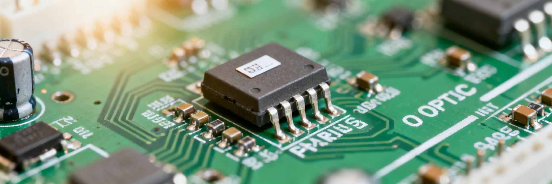
Pinout, package & absolute limits (data analysis)
Pinout diagram interpretation and package notes
The device is commonly offered in small-outline packages (e.g., SOT-23-5). Pinout interpretation: identify IN+, IN−, V+, V−/GND, and OUT pins; note any NC or substrate pins and the exposed thermal pad. Footprint cautions: ensure the exposed pad is handled per the recommended land pattern and use solder-mask-defined pads to control solder fillet. Guarding and short traces at IN+ and IN− drastically reduce leakage and measurable offset.
Absolute maximum ratings vs. recommended operating conditions
Extract absolute maximum voltages (e.g., supply to −0.3 V to +6.5 V), input protection clamps, ESD class and recommended temperature ranges; always allow safety margins (20–30%) in system transient analysis. Checklist for BOM/system review: confirm supply transient limits, input pin clamp currents, and ESD rating; validate that expected system transients (hot-plugging, inductive loads) won’t exceed device absolute maximums and cause latch-up or permanent shift.
Electrical performance deep-dive — what the datasheet really means (method/guide)
DC performance: offset, bias, and drift behavior
Offset and drift are measured using low-noise instrumental setups after long thermal soak; chopper stabilization reduces low-frequency offset and 1/f noise but can introduce clock feedthrough artifacts in some measurements. Input bias currents interact with source impedance to create DC errors; with 1 pA bias and 100 kΩ source, expect ~0.1 µV error, negligible for most systems. Measurement sensitivity: use guarded fixtures, thermal isolation, and long averaging to reach datasheet-level resolution.
AC/dynamic specs: bandwidth, noise, stability and output drive
Slew rate and GBW determine how the amplifier will behave driving capacitive loads or forming filters. For example, a 0.5 V/µs slew limits maximum step rates in sensor interfaces; a 1 MHz GBW imposes gain-dependent bandwidth constraints for active filter design. Noise density translates to RMS noise across the system bandwidth and sets ADC LSB requirements; design filters and gain to ensure amplifier noise doesn’t dominate the system noise budget.
Benchmarks & practical test procedures (benchmarks/case)
Suggested bench setups
Offset and drift: use a low-noise source, shorted inputs via guarded short, thermal soak for 30–60 minutes, then record offset over time and temperature. Input bias: apply a known source impedance and measure resulting DC error. Noise: measure with a low-noise preamp and spectrum analyzer. Recommended conditions: Vs = 5 V, RL = 10 kΩ, Ta = 25°C.
Common deviations
Common deviations include higher offset after poor layout, elevated noise from supply ripple, and lower output swing under heavy load. Typical reconciliation: add decoupling close to V+, reroute sensitive traces. Case study: an observed 30 µV offset was traced to a 2 MΩ leakage path from flux residues—cleaning corrected the shift.
Design checklist & application tips for reliable integration (action)
PCB/layout, power, and decoupling best practices
Prioritize decoupling: place 0.1 µF ceramic and 1 µF bulk within 1–2 mm of supply pins. Route IN+ and IN− as short, parallel, and shielded traces; avoid vias in the input path. Use a single-point star from amplifier ground to ADC ground; deploy guard rings on high-impedance nodes. Thermal considerations: keep the exposed pad soldered for stable thermal performance.
Substitution guidance and failure modes
When substituting, match offset, drift, input bias, RRIO behavior, and quiescent current first. Expected field failure modes include input overstress from transients and latch-up from exceeding absolute max supplies. Production tests: simple DC param test (Vcc, offset, bias) plus a functional sensor-in-loop check before assembly acceptance.
Summary
- The TP5531U-CR delivers the combination of low-offset, zero-drift behavior and low quiescent current suitable for precision, low-power front ends; verify performance under your system Vs and RL conditions.
- Key bench steps: guarded offset measurement after thermal soak, noise spectrum assessment with a low-noise chain, and dynamic tests (slew/bandwidth) with representative loads and filters.
- Layout and decoupling are decisive: close 0.1 µF+1 µF decoupling, guarded high-Z nodes, and proper exposed-pad soldering reduce deviations from datasheet numbers.
FAQ
What test setup validates TP5531U-CR offset and drift?
Use a guarded short for inputs, thermal soak the device for 30–60 minutes at target Ta, measure with a nanovoltmeter or high-resolution ADC, and log offset versus time and temperature. Use averaging and shielding to reach datasheet-level repeatability.
How does the pinout affect layout for the TP5531U-CR?
Identify IN+, IN−, V+, V−/GND and OUT pins on the package. Place decoupling adjacent to supply pins, keep input traces short and guarded, and ensure the exposed pad is soldered to the PCB thermal land to stabilize offsets and dissipate heat.
Which datasheet parameter should be prioritized for battery-powered precision sensors?
Prioritize quiescent current, input offset/drift, and RRIO performance. Quiescent current affects battery life; offset and drift determine long-term accuracy; RRIO ensures full-scale measurement on single supplies. Validate all three during incoming test and system integration.


