
A professional guide for designers to prioritize DC/AC parameters in low-power analog front ends.
Across published datasheets for the LM358 family, designers repeatedly face a trade-off: low quiescent current and wide single-supply range versus modest bandwidth and limited slew rate. This introduction outlines how to read a typical LM358A-SR datasheet, prioritize the DC and AC numbers that affect system behavior, and use quick benchmarks to decide if the part fits a low-power analog front end.
Practical designers use a short, repeatable reading pattern—scan absolute limits, recommended conditions, electrical tables, and typical curves—then verify with bench tests. The following sections walk that process step by step, focusing on the parameters that determine sensor conditioning, low-frequency filtering, and comparator-like uses.
Background — LM358A-SR Overview & Typical Use Cases
Functional summary and intended applications
Point: The LM358A-SR is a dual, single-supply operational amplifier optimized for low-power tasks. Evidence: Datasheet tables present dual-channel configurations with input stage and output stage limitations versus rail‑to‑rail parts. Explanation: That architecture makes it well suited to sensor conditioning, low‑frequency active filters, level shifting, and simple comparator replacements when speed and rail‑to‑rail output are not required.
Datasheet sections to scan first
Point: Start reading the Absolute Maximum Ratings, Recommended Operating Conditions, Electrical Characteristics, Typical Performance Curves, and Application Notes. Evidence: Those sections contain limits, test conditions, and curves that determine safety margins and expected behavior. Explanation: Scanning them first reduces design risk by revealing temperature limits, supply ranges, test voltages, and the conditions under which key numbers (offset, GBW, slew) were measured.
Data Analysis — Datasheet Deep-Dive: Key Specs to Extract
DC parameters (what to record and why)
Point: Record input offset voltage, input bias/current, input common‑mode range, output swing, and quiescent current per channel. Evidence: Electrical tables list these values under specific Vcc, temperature, and load conditions. Explanation: Offset affects low‑gain sensor amplifiers, bias current drives error with high‑impedance sensors, common‑mode range governs single‑supply sensing near ground, output swing limits define headroom, and quiescent current sets power budget.
AC parameters and stability indicators
Point: Extract gain‑bandwidth product (GBW), slew rate, open‑loop gain, phase margin/compensation notes, CMRR and PSRR. Evidence: Typical performance curves and AC characteristic tables provide GBW and slew rate test points and show load‑dependent behavior. Explanation: GBW and slew rate determine closed‑loop bandwidth and transient response; CMRR/PSRR affect accuracy in noisy or varying supply environments, and compensation notes indicate required closed‑loop gains for stability.
Benchmarks — Benchmarks & Typical Ranges for LM358A-SR
Point: Expect a wide single‑supply range, low hundreds of microamps quiescent per amplifier, ~1 MHz GBW, and modest slew rate. Evidence: Most LM358A‑type datasheets list single‑supply operation from low single digits up to tens of volts, typical quiescent currents near 250–700 μA per channel, GBW around 0.7–2 MHz, and slew rates on the order of 0.2–0.6 V/μs.
| Parameter | Typical | Worst‑case (from tables) |
|---|---|---|
| Supply range | Single 3 V – 32 V | Must remain within Absolute Maximums |
| Quiescent current / channel | ~250–700 μA | Up to ~1 mA at extremes |
| GBW | ~0.7–1.5 MHz | Lower at high load / temp |
| Slew rate | ~0.2–0.6 V/μs | Can be lower with heavy loading |
| Input offset | 1–5 mV typical | Tens of mV in worst case |
Application-driven benchmark: For a sensor amplifier covering 10 Hz–10 kHz, a GBW ≥10× closed‑loop gain is recommended. With GBW ~1 MHz, closed‑loop gains up to 100 give usable bandwidth into the tens of kilohertz when slew and phase margin are acceptable.
Audio Context: For a low‑frequency audio preamp, noise and distortion may be acceptable at modest gains. Use cautious filtering and ensure supply decoupling to avoid noise injection when the op amp is used in audio LF paths.
Method / How-to — Design & Bench Testing Guide
PCB layout, decoupling, and recommended circuit practices
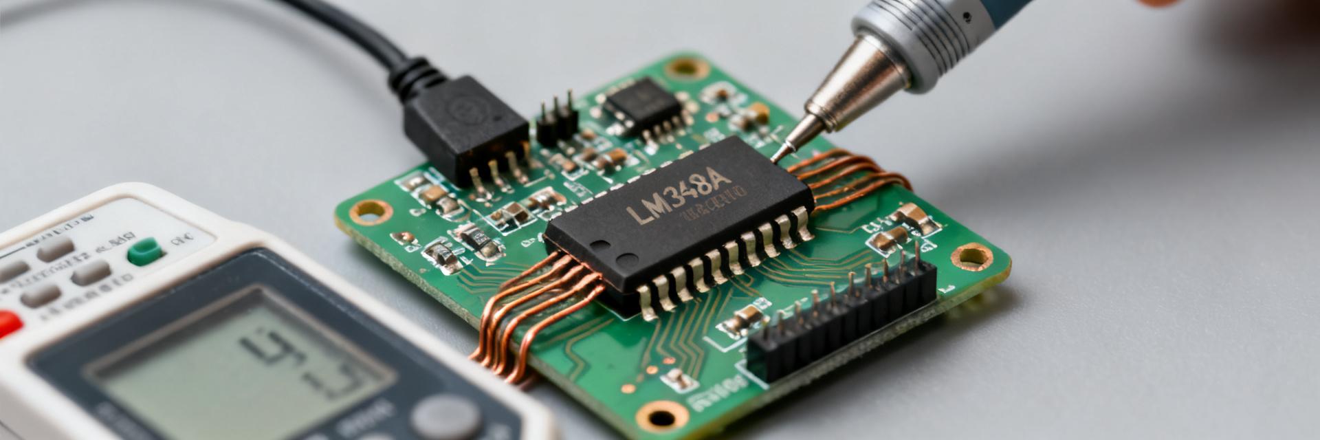
Point: Good layout and bypassing are critical to match datasheet performance. Evidence: Measurement discrepancies often trace to inadequate supply bypass, long input traces, or unshielded high‑impedance nodes. Explanation: Use a 0.1 μF ceramic plus a 1 μF bulk on the supply pins, short ground returns, guard traces for high‑Z inputs, series input resistors for protection, and place the op amp close to the sensor interface to minimize leakage and parasitics.
Measurement checklist and test setups
Point: Validate offset, bias, GBW, slew, and output swing with repeatable setups. Evidence: Simple tests—DC offset with high‑resolution DVM and low‑noise supply, input bias via large resistor and offset calculation, GBW with closed‑loop gain and swept sine, slew with large step input—map directly to datasheet claims. Explanation: Use calibrated probes, known loads (e.g., 2 kΩ), and the same supply and temperature conditions as the datasheet to assess pass/fail thresholds.
Actionable — Selection Checklist & Trade-offs
Quick selection checklist
- Supply voltage fits within the device single‑supply range and headroom needs are met.
- Required bandwidth is modest (tens of kHz to low hundreds of kHz in closed‑loop).
- Offset and input bias tolerances match the sensor and gain requirements.
- Power budget supports ~0.3–1 mA per amplifier.
- Output drive and rail excursion are adequate for the load.
Practical trade-offs
Point: Common trade‑offs are power versus speed and offset versus cost. Evidence: Higher‑speed, rail‑to‑rail, or low‑offset alternatives incur more quiescent current or higher BOM cost. Explanation: When substituting, compare GBW, slew rate, input offset/bias, output swing curves, and repeat the bench checklist.
Summary
- The LM358A-SR is a practical choice when low quiescent current and single‑supply operation are priorities; check the datasheet tables for exact DC and AC limits.
- Key specs: input offset, input bias, common‑mode range, output swing, quiescent current, GBW, and slew rate—these determine suitability for sensor conditioning.
- Validate datasheet claims on the bench and use proper PCB decoupling to avoid measurement errors.
Frequently Asked Questions
What datasheet sections are most critical for LM358A-SR selection?
Focus on Absolute Maximum Ratings, Recommended Operating Conditions, Electrical Characteristics, and Typical Performance Curves. These reveal safe limits, the exact test conditions for each spec, and typical behavior under load.
How do I test GBW and slew rate for the LM358A-SR?
Measure closed‑loop response with a known gain and a swept sine to find −3 dB bandwidth. For slew rate, apply a large fast step and measure output slope; keep load and supply matching datasheet test conditions.
When should I avoid using the LM358A-SR?
Avoid it if you need >1 MHz GBW, fast slew (>1 V/μs), true rail‑to‑rail output, or ultra‑low input offset/bias. In those cases, opt for high-speed or precision specified op amps.


