
In-depth technical analysis for high-voltage precision applications.
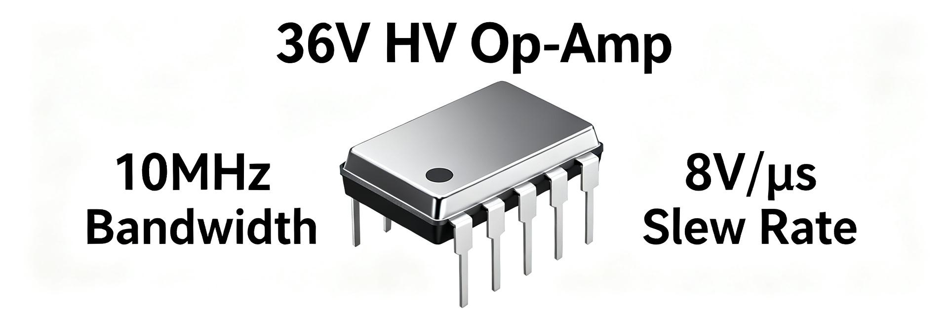
The TP2584-SR targets high-voltage precision applications by combining a wide supply capability (up to ≈36 V), a unity-gain bandwidth near 10 MHz, and a slew rate around 8 V/µs. You’ll find these datasheet figures point the device toward sensor front-ends and high-voltage buffering: the GBW and slew-rate pairing supports moderate-speed signals, while the voltage headroom enables single-supply measurement chains. This report translates those datasheet numbers into practical expectations, measurement methods, and design guidance you can apply on the bench and in prototypes.
1 — Background: Why the TP2584-SR matters for high-voltage op-amp designs
Key datasheet-rated specs at a glance
Point: The device is specified for high-voltage operation and moderate bandwidth. Evidence: datasheet callouts include supply range to ≈36 V, GBW ≈10 MHz, slew ≈8 V/µs, input offset in low-mV range, input bias in nA to pA range (typical), output swing within a few volts of rails, and supply current in the low mA range. Explanation: these numbers mean you get substantial headroom for sensor excitation and buffering while retaining reasonable closed-loop bandwidth for gains >1.
| Parameter | Typical / Range | Design implication |
|---|---|---|
| Supply voltage | Up to ≈36 V | Supports single-supply high-voltage sensors and +/- configurations |
| Unity-gain BW | ≈10 MHz | Closed-loop BW scaled by gain (see examples below) |
| Slew rate | ≈8 V/µs | Limits large-signal step settling and output slew |
| Input offset / bias | mV / nA–pA | Offset budgeting critical for precision front-ends |
Typical target applications and design contexts
Point: The spec set aligns with several application classes. Evidence: moderate GBW plus high-voltage capability maps to sensor front-ends, HV buffers, precision amplifiers, and moderate-speed data acquisition. Explanation: you should choose TP2584-SR where you need rail-to-rail headroom or high supply voltage, modest closed-loop bandwidth (kHz–low MHz), and decent transient performance, while avoiding ultra-high-speed or microsecond-scale precision pulse applications.
2 — Electrical performance deep-dive: Datasheet specs interpreted
Frequency, slew, and transient behavior (what the numbers imply)
Point: GBW and slew rate jointly determine small-signal BW and large-signal settling. Evidence: with GBW ≈10 MHz you can expect closed-loop bandwidth roughly GBW/G; for gains of 1, 5, and 10 that yields ~10 MHz, 2 MHz, and 1 MHz respectively, while 8 V/µs slew limits maximum fast-edge amplitude before slew-dominated distortion. Explanation: in gain-of-1 buffering you’ll approach the device’s GBW, but at gain 10 the bandwidth is constrained; for large steps, calculate required slew = ΔV/edge_time to verify the op amp can settle within required time.
Noise, offset, input/output limits and DC performance
Point: DC parameters set precision floor and dynamic SNR. Evidence: the datasheet lists input-referred offset in the low-millivolt range, drift modest under temperature, input bias currents typically in the nA–pA band, and output swing within a few volts of rails depending on load. Explanation: plan offset-cancellation or calibration for sub-millivolt systems, budget input bias contribution for high-impedance sources, and ensure ADC input headroom if you rely on the op amp’s output swing near rails.
3 — Test bench & measured metrics: Turning datasheet into lab expectations
Recommended test setup & measurement methods
Point: Reproduce datasheet conditions to validate performance. Evidence: use clean ± or single rails up to device limits, 1 kΩ load or specified load, proper bypassing (0.1 µF ceramic plus 10 µF bulk close to supply pins), and short feedback traces. Explanation: measure frequency response with small-signal excitation (10–20 mV), capture slew with large-step pulses (e.g., 2–10 V steps), and verify PSRR/CMRR with differential sources; document all conditions when comparing to datasheet.
Typical measured results, tolerances and failure modes to watch
Point: Lab results often deviate due to layout and temperature. Evidence: expect measured GBW to vary by ±10–20% from nominal, offset drift increase under thermal stress, and slew/settling impacted by supply decoupling. Explanation: common failure signatures include low-frequency oscillation from long feedback traces or insufficient bypassing, thermal limiting when dissipating significant power, and degraded PSRR when supplies are noisy—addressable with layout fixes and thermal management.
4 — Comparative use-cases & design examples (practical blueprints)
Example A — High-voltage sensor front-end (schematic + rationale)
Point: For sensor excitation and measurement you need input protection and controlled gain. Evidence: implement series input resistor (1–10 kΩ) and clamp/protection network, set noninverting gain via Rf/Rg for desired sensitivity, and add a small feedback capacitor (1–10 pF) for stability if capacitive loads present. Explanation: the network trades off bandwidth vs. stability and noise; choose R values to limit input current and preserve SNR, and buffer outputs if driving cables or ADCs.
Example B — Precision buffer for data-acquisition chain
Point: A buffer stage isolates source and drives ADC inputs reliably. Evidence: use unity or low gain, keep source impedance Explanation: prioritize layout and decoupling to minimize offset and settling; for fast successive approximation ADCs, ensure the buffer’s settling meets ADC acquisition time and the slew won’t introduce conversion error.
5 — Practical recommendations & design checklist for deploying TP2584-SR
Layout, decoupling, and thermal best practices
Point: PCB practices directly affect achievable performance. Evidence: place bypass caps within 2–3 mm of supply pins, use a solid ground return, keep feedback loop traces short, and add thermal vias under package if dissipating >200–300 mW. Explanation: these steps reduce oscillation risk, preserve PSRR and CMRR, and prevent thermal drift; compute power dissipation from (Vsupply × Iq + load losses) and confirm package PD limits in worst-case ambient temperatures.
When to rely on the datasheet vs. when to prototype: risk checklist
Point: Use the datasheet for initial selection but validate critical behaviors in hardware. Evidence: rely on datasheet for static limits and expected ranges, but prototype when circuit margins are tight (bandwidth, noise, offset, or thermal). Explanation: prioritize frequency response, large-signal settling, and PSRR tests during prototyping; red flags include oscillation, unexpected offset shifts, or thermal shutdown—any of which require layout, component, or topology changes.
Summary
- TP2584-SR offers ~36 V supply capability, ≈10 MHz GBW and ~8 V/µs slew, making it suited for high-voltage buffering and sensor front-ends where moderate bandwidth and high headroom matter.
- Performance hinges on layout and decoupling: expect GBW variance of ±10–20% and slew-limited settling on large steps; validate these with the recommended bench tests and small-signal Bode and step measurements.
- Design checklist: short feedback traces, close bypassing, input protection for sensors, and power dissipation verification before qualifier runs to ensure reliable operation.
FAQ
How should you verify the TP2584-SR bandwidth and slew on the bench?
Measure small-signal frequency response with a network or impedance analyzer using a 10–20 mV sine input to extract GBW and phase margin, then apply a large amplitude step (2–10 V) to capture slew and large-signal settling. Record supply rails, load, and temperature to match datasheet conditions and note deviations.
What test conditions most strongly affect measured offset and noise?
Input source impedance, supply cleanliness, and temperature are primary factors. Use low-noise references, shielded probes, and proper bypassing; measure input-referred noise with a low-noise preamp or spectrum analyzer, and perform offset drift tests over the expected ambient range to validate calibration needs.
When is a prototype mandatory despite strong datasheet numbers?
Prototype when margins are tight—if your application demands near-rail output swing, sub-millivolt offset, or high-speed settling for ADC timing. Also prototype when board layout constrains trace lengths or thermal dissipation could approach package limits; real-world layout often reveals issues not obvious from datasheet figures.


