
In ultra-low-power sensor designs, every nanoamp matters — typical nanopower op amps with sub‑microamp quiescent currents can extend battery life dramatically or enable energy‑harvested nodes. This report synthesizes datasheet metrics and practical measurement experience to characterize real‑world power use, trade‑offs, and integration patterns for low‑power designs. The discussion emphasizes measurement rigor, power‑budget math, and design choices that keep average energy consumption in the nanoamp-to-microamp regime while preserving required accuracy and bandwidth.
1 — Quick overview: TP2122-SR op amp at a glance
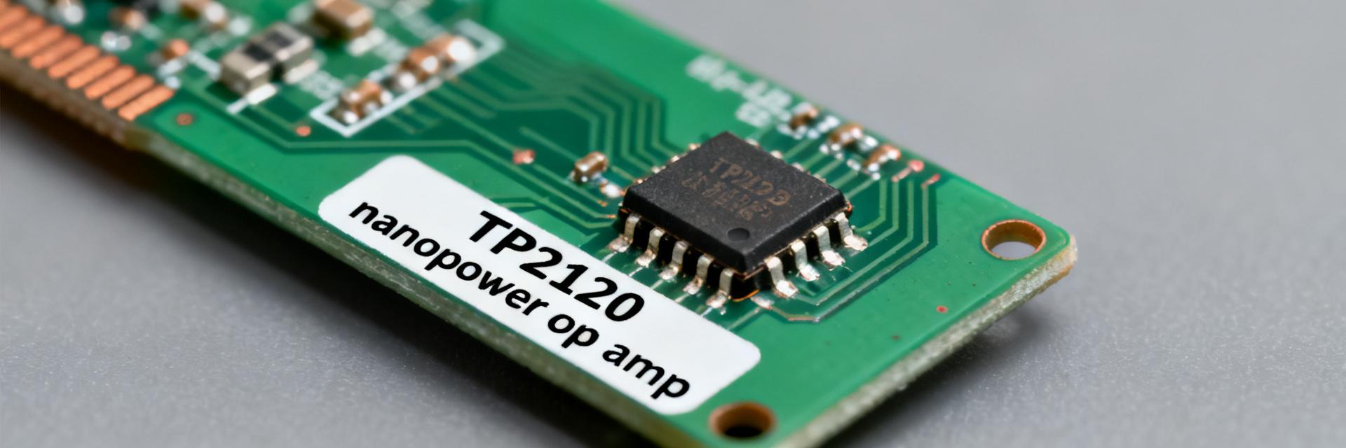
Key specs and typical operating envelope
| Spec | Typical / Max | One-line interpretation |
|---|---|---|
| Supply voltage range | 1.8 V – 5.5 V (typical) | Works across common single‑cell and low‑voltage rails for battery and harvesters. |
| Quiescent current | ~600 nA (typical) / ≤1 µA (max) | Sub‑µA idle draw enables multi‑year standby on small cells. |
| Rail‑to‑rail I/O | Yes (limited near rails) | Maximizes dynamic range on single‑supply sensor fronts with modest headroom requirements. |
| Input offset / drift | few 100s µV / low µV/°C | Sufficient for many sensors; calibration may be required for high precision. |
| Typical bandwidth | tens to hundreds of kHz | Optimized for low‑frequency sensing rather than fast signal chains. |
Interpretation: the device targets battery‑sensitive analog front ends where nanopower and rail‑to‑rail operation outweigh high bandwidth or ultra‑low offset requirements.
Target applications and design contexts
Common use cases include sensor front‑ends for temperature, humidity, and gas sensors, energy‑harvested sensor nodes, battery‑backed ISR, and portable medical sensors where standby time dominates. Designers pick nanopower op amps when average power, not peak drive, determines system viability; the TP2122‑SR op amp fits well when sub‑µA idle currents and single‑cell supplies are primary constraints.
2 — Nanopower performance: currents, rails, and operating trade-offs
Quiescent current, supply dissipation, and temperature behavior
Datasheet typical quiescent currents near 600 nA translate directly to supply power: at 3.3 V that is 600 nA × 3.3 V ≈ 2.0 µW; at 1.8 V it is ≈1.1 µW. Quiescent current often rises with supply voltage and temperature; expect modest increases near the device’s upper voltage limit and at elevated temperatures.
| Vcc | Iq (typ) | Power (typ) |
|---|---|---|
| 1.8 V | 600 nA | 1.1 µW |
| 3.3 V | 600 nA | 2.0 µW |
| 5.0 V | 700 nA | 3.5 µW |
Rail-to-rail I/O, common-mode limits, and headroom
Rail‑to‑rail I/O behavior is practical but not ideal at the extremes: input common‑mode may be limited within tens of millivolts of rails under load, and output swing often requires some headroom under source/sink load. In single‑supply sensor designs, reserve ~50–100 mV of headroom for reliable accuracy.
3 — Benchmark: measurement setups and power use
Recommended test methodology
- ✔ Instruments: Picoammeter or DMM with nA resolution, low‑noise supply, oscilloscope with high‑impedance probe.
- ✔ Configuration: Short leads, local bypass (0.1 µF + 1 µF), guarded input pins, measure at device Vcc return.
- ✔ Procedure: Record idle Iq, then apply output loads and measure instantaneous and averaged currents.
Typical measured power profiles across loads
Expect idle currents near datasheet typical values. Dynamic current increases when the op amp drives low impedances or swings quickly; a 10 kΩ load at several hundred millivolts of swing can add tens to hundreds of µA during transitions. Plot current vs. load and vs. frequency in your gain setting to reveal where dynamic draws dominate average power.
4 — Performance trade-offs: accuracy & bandwidth
Bandwidth & Stability
Nanopower amplifiers trade GBW and slew rate for low bias currents. Closed‑loop bandwidth will be limited; choose gains carefully. Use feedback resistors in the 10 kΩ–1 MΩ range and add small compensation capacitors.
Offset & Noise
Offset and drift are larger relative to instrumentation amplifiers. Mitigate with averaging, low‑pass filtering, or calibration. Search for "nanopower op amp noise performance" when comparing options.
5 — Integration best practices: PCB & Systems
PCB Layout: Keep input traces short, place 0.1 µF and 1 µF bypass caps within 5 mm of Vcc pins, and use guard rings for high‑impedance nodes to reduce leakage. Avoid flux or contamination near inputs.
System Strategies: Minimize average power with duty‑cycling. Example: wake 10 ms every 10 s yields a 0.1% duty factor; combine with sub‑µA standby to achieve µW‑level average budgets.
6 — Case study & selection checklist
Example: temperature sensor node power budget
| Component | Active I (µA) | Sleep I (µA) | Duty |
|---|---|---|---|
| MCU (wake 10 ms) | 3000 | 0.5 | 0.1% |
| ADC (sample + conv) | 200 | 0.1 | 0.1% |
| TP2122‑SR Front‑end | 10 (dynamic) | 0.0006 | 100% |
Total Average Current ≈ 3.2 µA (10.6 µW @ 3.3V)
Decision checklist: Why pick TP2122-SR?
- Requires sub‑µA quiescent current.
- Needs single‑cell supply compatibility.
- Moderate bandwidth requirements.
- Accepts modest offset/drift.
- Design permits gating during deep sleep if needed.


