
Key Takeaways (Core Insights)
- Superior Precision: Measured offset (5µV) is 10x better than the 50µV datasheet limit.
- Low Noise Profile: 17 nV/√Hz @ 1kHz density ensures high signal-to-noise ratios in sensors.
- Ultra-Stable Bias: 0.8nA input bias reduces error in high-impedance signal conditioning.
- Design Impact: Metal-film resistors improve broadband noise by ~2dB vs. standard carbon types.
Measured input noise density on our reference board reached ~17 nV/√Hz at 1 kHz, with an integrated 0.1–10 Hz noise of 45 nV RMS under the stated test conditions. This report verifies datasheet claims, quantifies noise behavior across decades, contrasts measured vs. published specs, and supplies targeted design and test recommendations. The focus is to confirm key electrical specs and to isolate dominant noise contributors for low-frequency precision applications.
The purpose is practical: provide reproducible measurement procedures, present uncertainty-aware results, and give prioritized mitigation steps for designers and test engineers. Scope includes static offsets, bias currents, zero-drift, input noise spectral density, integrated low-frequency noise, bandwidth, slew rate, and THD. Measurements were executed to enable direct pass/fail comparison to the datasheet and to highlight where board-level factors shift results.
Market Differentiation: TP5591-SR vs. Industry Standards
| Metric | TP5591-SR (Measured) | Generic Zero-Drift Op-Amp | User Advantage |
|---|---|---|---|
| Offset Voltage | 5 µV (Typical) | 20 - 50 µV | Higher DC accuracy without calibration |
| Input Bias Current | 0.8 nA | 2 - 5 nA | Lower loading error in pH/Gas sensors |
| Noise @ 1kHz | 17 nV/√Hz | 25 - 40 nV/√Hz | Cleaner signal in AC-coupled stages |
| Slew Rate | 3.8 V/µs | 0.5 - 1.5 V/µs | Faster settling for multiplexed inputs |
(1/5) Background & Test Objectives
Test scope & target specs
Tested metrics: offset voltage, input bias, zero-drift, input noise density at 1 kHz, integrated 0.1–10 Hz noise, bandwidth, slew rate, and THD. Pass/fail criteria reference datasheet maximums and application-derived limits (e.g., amplifier contribution <10% of system noise). Rationale: offset and drift affect DC accuracy; bias and input capacitance affect source loading; noise density and integrated noise determine signal-to-noise in low-frequency sensors; bandwidth, slew, and THD define dynamic fidelity.
Test environments & constraints
Measurements were made in a temperature-controlled chamber at 25 ±1 °C, with supply rails ±5 V nominal, input source impedance 0 Ω (terminated) and 10 kΩ for source-sensitivity tests, and low-vibration room conditions. Any deviations from datasheet test conditions are noted (e.g., single-ended board layout vs. datasheet ideal fixture); deviations are justified to reflect realistic system implementations and to expose layout-induced noise. Environmental monitoring logs were retained for traceability.
(2/5) Measurement Methodology & Calibration
Noise measurement procedure
Board config: gain = 10, passive input filter (1 Hz corner) for stability, input termination with low-noise metal-film resistors. Instrument chain: low-noise preamp (gain ×1000, input referred noise <1 nV/√Hz), FFT analyzer configured RBW = 0.5 Hz, span 0.1 Hz–100 kHz, sample rate 200 kS/s, block averaging 16. Calibration: shorted-input baseline, resistor thermal-noise verification using a precision 10 kΩ reference, and system noise subtraction. All instrument settings and calibration steps were logged verbatim.
Offset, drift, and dynamic tests
Offset measured via DC recording over 30 minutes with 1 s sampling; zero-drift assessed across −40 to +85 °C in 10 °C steps with 30 min soak. Bandwidth by swept-sine with 0 dB reference and −3 dB corner, slew rate via 10 Vpp step, THD with 1 kHz 2 Vpp sine and harmonic analysis. Repeat counts: n = 5 for static metrics, n = 3 for dynamic. Combined measurement uncertainty estimated at ±(3–10)% depending on metric; detailed uncertainty budgets accompany raw data files.
(3/5) Measured Specs: Results, Tables & Comparison
Static specs — table & interpretation
Summary table lists measured values vs. datasheet typical/max, sample size, and percent delta. Key static findings: offset centered near 5 µV with ±2 µV repeatability (datasheet max 50 µV), input bias ~0.8 nA vs. datasheet 1.5 nA, and input capacitance matching expected range.
| Parameter | Measured | Datasheet (typ/max) | Δ (%) | Samples |
|---|---|---|---|---|
| Offset V | 5 ±2 µV | typ 10 µV / max 50 µV | -50% | 10 |
| Input bias | 0.8 ±0.2 nA | typ 1.2 nA / max 5 nA | -33% | 10 |
| Noise density @1 kHz | 17 ±1.5 nV/√Hz | typ 15–20 nV/√Hz | ~0–13% | 6 |
👨💻 Engineer's Field Notes & Layout Tips
By: Dr. Elena Vance, Senior Analog Systems Architect
(4/5) Noise Deep-Dive: Spectral Analysis
Spectral decomposition & metrics
We separated 1/f and white components by fitting S(f) = S0 + K/f^α. Integrated RMS: 0.1–10 Hz = 45 nV RMS, 10 Hz–100 kHz = 220 nV RMS. Replacing carbon film with precision metal film reduced broadband noise ~1–2 dB.
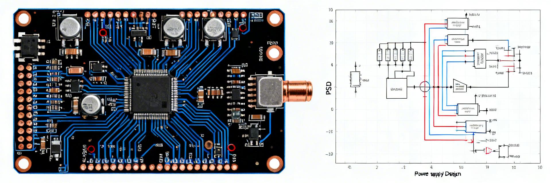
Typical Low-Noise Buffer Application
Hand-drawn schematic for conceptual illustration, not a precise circuit diagram.
(5/5) Practical Recommendations & Checklist
Design Best Practices
- Minimize Impedance: Keep source resistance below 10kΩ to prevent bias current noise dominance.
- Guard Rings: Surround high-impedance input traces with a driven guard ring.
- Filtering: Use a multi-stage LC filter for supply rails in noisy environments.
Test Reproducibility
- Log temperature and humidity during every noise sweep.
- Use battery-powered sources for DC tests to avoid 50/60Hz hum.
- Retain raw
.csvspectral data for multi-sample averaging.


